Pixel Structure and Method for Manufacturing the Same

Active Publication Date: 2009-04-30
AU OPTRONICS CORP
View PDF2 Cites 29 Cited by
  • Summary
  • Abstract
  • Description
  • Claims
  • Application Information

AI Technical Summary

Benefits of technology

[0014]One objective of this invention is to provide a pixel structure and a method of manufacturing the same which requires only six photolithography-etc

Problems solved by technology

However, there are still some image display problems in L

Method used


Image

  • Pixel Structure and Method for Manufacturing the Same
  • Pixel Structure and Method for Manufacturing the Same
  • Pixel Structure and Method for Manufacturing the Same

Examples


second embodiment

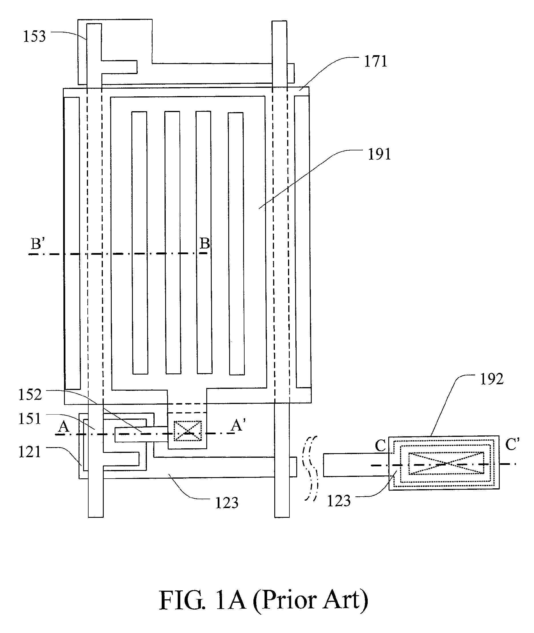
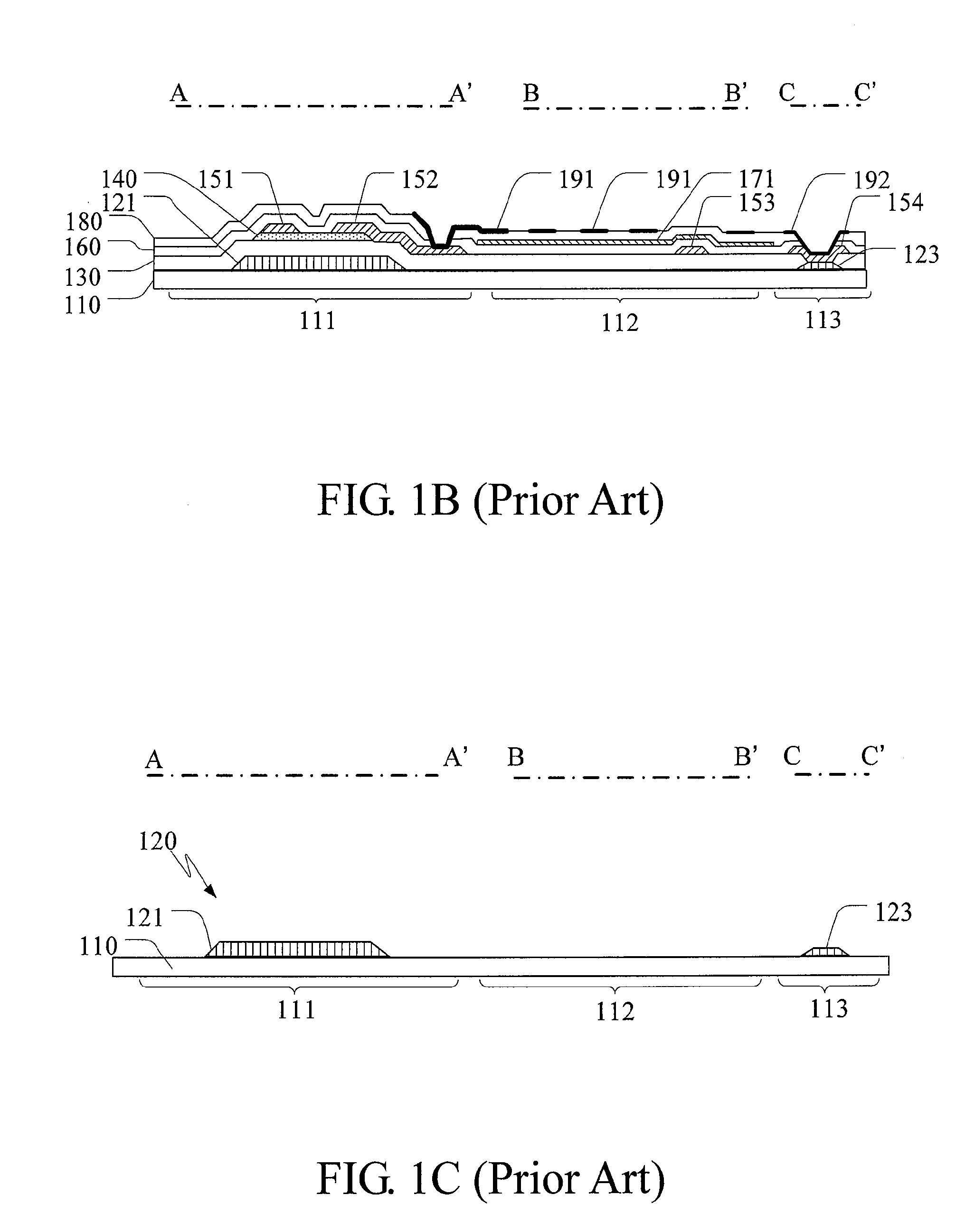
[0038]In reference to FIG. 3A and FIG. 3B, there is a method for manufacturing a pixel structure in accordance with this invention and the pixel structure thus formed. The pixel structure comprises a control area 311 and a display area 312. The manufacturing method thereof disclosed in this embodiment is shown in FIGS. 3C to 3H. For convenience, FIGS. 3B to 3H are depicted as cross-sectional views taken along lines A-A′, B-B′ and C-C′ in FIG. 3A.

[0039]As shown in FIG. 3C, in the first photolithography-etching process of this embodiment, a patterned first conductive layer 320 is formed on the substrate 310, in which the patterned first conductive layer 320 comprises a data line 322 and a gate electrode 321. It should be noted that, as can be readily understood from the cross-sectional lines shown in FIG. 3A, the gate electrodes 321 depicted in FIG. 3C are a single electrode structure, and they are shown separately to disclose the concept of this invention more clearly. This is also t...

first embodiment

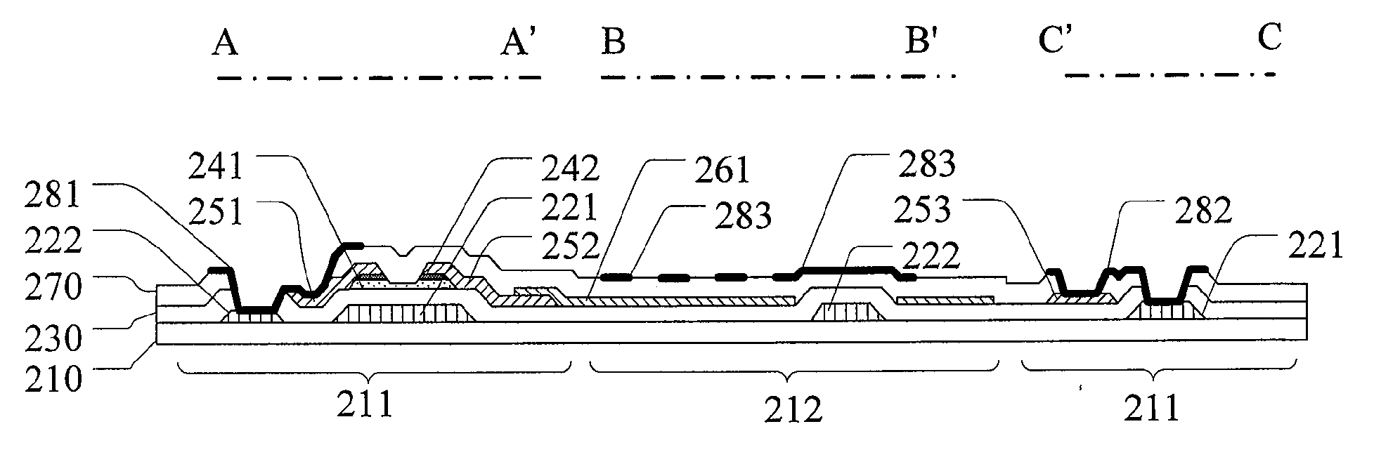
[0047]The pixel structure formed in this embodiment by the manufacturing process described above differs slightly from the pixel structure of the In this embodiment, the pixel electrode 383 is formed on the second insulating layer 370, has a plurality of slits, and is electrically connected to the drain electrode 352 of the TFT structure, while the common electrode 361 is formed beneath the second insulating layer 370. Similarly, the common electrode 361, the data line connecting electrode 381 and the gate line connecting electrode 382 all can be formed simultaneously in a single process. As a result, the pixel structure of this embodiment can be completed by only six photolithography-etching processes.

[0048]It follows from the above description that as compared to conventional technologies, which require seven photolithography-etching processes, the pixel structure of the FFS-LCD utilizing this invention requires only six photolithography-etching processes, thus saving both manufa...


PUM


Abstract

A pixel structure of a fringe field switching liquid crystal display (FFS-LCD) and a method for manufacturing the pixel structure are provided. Compared to the conventional method of using seven photolithography-etching processes for manufacturing a pixel structure, the method of the present invention uses only six photolithography-etching processes that save manufacturing costs and time. Furthermore, the pixel structure thereby only comprises two insulating layers, and thus, the light transmittance thereof can be increased in comparison to the conventional pixel structure comprising three insulating layers.

Description

[0001]This application claims priority to Taiwan Patent Application No. 096141108 filed on Oct. 31, 2007, the disclosures of which are incorporated herein by reference in their entirety.CROSS-REFERENCES TO RELATED APPLICATIONS[0002]Not applicable.BACKGROUND OF THE INVENTION[0003]1. Field of the Invention[0004]The present invention provides a pixel structure and a manufacture method for use in a liquid crystal display (LCD), specifically, in a fringe field switching LCD (FFS-LCD).[0005]2. Descriptions of the Related Art[0006]Among all kinds of display products currently available, the liquid crystal display (LCD) is becoming the mainstream product. However, there are still some image display problems in LCDs, such as slow response speed and low aperture ratios. To overcome such problems, a fringe field switching LCD (FFS-LCD) has been proposed, which, compared to the conventional in-plane switching LCD (IPS-LCD), has an improved aperture ratio, a better overall light transmittance, a...

Claims


Application Information

Patent Timeline
IPC IPC(8): H01L27/12H01L21/84
CPCG02F1/134363H01L27/1214G02F2001/134372G02F1/134372H01L27/124H01L27/1288
Inventor LIN, HSIANG-LINLIN, CHING-HUAN
Owner AU OPTRONICS CORP
Why Eureka
Try Eureka