Light-Emitting Device

a light-emitting diode and light-emitting technology, which is applied in the direction of semiconductor devices, electrical equipment, basic electric elements, etc., can solve the problems of photons easily reflected and trapped in the semiconductor, and achieve the effect of enhancing the lighting efficiency of the light-emitting diod

Inactive Publication Date: 2009-05-07
NAT TAIWAN UNIV
View PDF5 Cites 38 Cited by
  • Summary
  • Abstract
  • Description
  • Claims
  • Application Information

AI Technical Summary

Benefits of technology

[0006]According to the issues described, the invention provides a method for enhancing lighting efficiency of a light-emitting diode by surface plasma coupling.

Problems solved by technology

However, photons are easily reflected and trapped in the semiconductor to change into heat and only a few photon parts can be radiated out of the light-emitting diode.

Method used


Image

  • Light-Emitting Device
  • Light-Emitting Device
  • Light-Emitting Device

Examples


Embodiment Construction

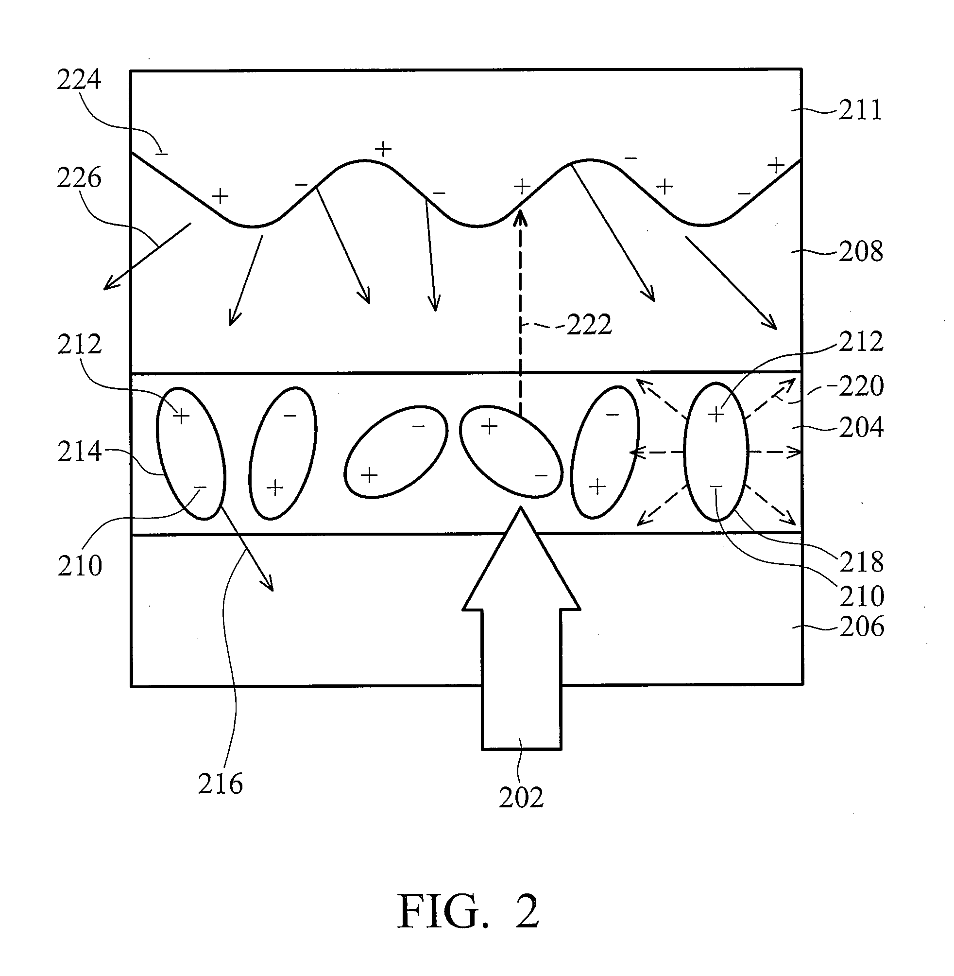
[0019]Referring to FIG. 2, which illustrates a mechanism for enhancing lighting efficiency of a light-emitting diode by surface plasmon coupling of an embodiment of the invention, an excitation 202, such as a current or laser, passes a bottom structure layer 206 of the light-emitting diode and injects into an active layer 204 to generate electrons 210 and holes 212. According to the design of the device structure, electrons 210 and holes 212 are then recombined in the active layer 204 to generate energy. Electrons 210 and holes 212 can be recombined in two ways, one is radiative recombination 214 and another is non-radiative recombination 218. Radiative recombination 214 generates photons 216 which are generally represented as light. Non-radiative recombination 218 generates phonons 220 which are generally represented as lattice vibration or heat. Most photons 216 are trapped in the structure layer and only a few parts can be radiated out of the light-emitting diode.
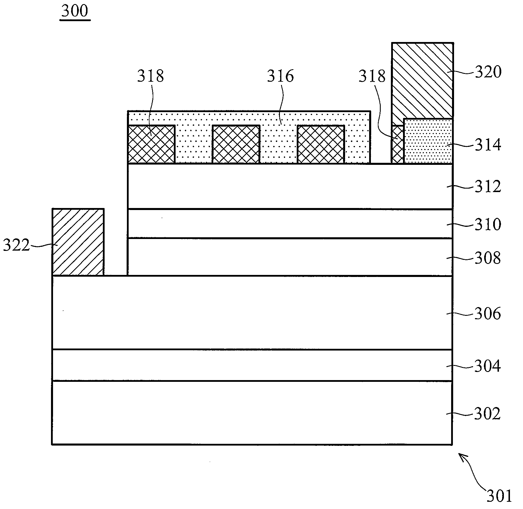
[0020]A light-em...


PUM


Abstract

The invention provides a light-emitting device, comprising a light-emitting element and a surface plasmon coupling element connected to the light-emitting element. In an embodiment of the invention, the surface plasmon coupling element comprises a dielectric layer connected to the light-emitting element and a metal layer on the dielectric layer. In another embodiment of the invention, the light-emitting device is a light-emitting diode, comprising an active layer between an n-type semiconductor layer and a p-type semiconductor layer, and a surface plasmon coupling element adjacent to the n-type semiconductor layer. In a further embodiment of the invention, a current spreading layer on a second type semiconductor layer of the light-emitting device includes a plurality of strip-shaped structures, and the surface plasmon coupling element is disposed on the current spreading layer and filled into the gap between the strip-shaped structures of the current spreading layer.

Description

BACKGROUND OF THE INVENTION[0001]1. Field of the Invention[0002]The invention relates to a light-emitting device and more particularly relates to a light-emitting diode.[0003]2. Description of the Related Art[0004]Semiconductor light-emitting devices have developed rapidly in many applications, for example liquid crystal display backlights. As such, semiconductor light-emitting devices may replace currently used illuminations, such as fluorescent lamps or light bulbs. Specifically, GaN based light-emitting diodes are the focus of white light sources and liquid crystal display backlights.[0005]FIG. 1 shows the structure of a conventional InGaN based light-emitting diode, which sequentially includes a buffer layer 104, an n-GaN layer 106, an InGaN / GaN quantum well structure 108, a p-GaN layer 110 and a transparent conductive layer 112 on a substrate 102. A p-type electrode 114 connects the transparent conductive layer 112 and an n-type electrode 116 connects the n-GaN layer 106. When ...

Claims


Application Information

Patent Timeline
Patent Type & Authority Applications(United States)
IPC IPC(8): H01L33/00H01L33/44
CPCH01L33/44
Inventor YANG, CHIH-CHUNGYEH, DONG-MINGCHEN, CHENG-YENLU, YEN-CHENGSHEN, KUN-CHINGHUANG, CHI-FENG
Owner NAT TAIWAN UNIV
Why Eureka
Try Eureka