Electro-optical device, manufacturing method of the same, and electronic apparatus

Active Publication Date: 2005-04-21
INTELLECTUAL KEYSTONE TECH LLC
View PDF12 Cites 29 Cited by
  • Summary
  • Abstract
  • Description
  • Claims
  • Application Information

AI Technical Summary

Benefits of technology

[0029] In the case of the surface protection layer which is formed on the upper side of the gas barrier layer via an adhesion layer containing fine particles, the film-thickness of the adhesion layer can be easily uniform, due to the fine particles. Also, the fine particles form an optical guide, and the light take-up efficiency can be enhanced. When the fine particle are flexible material, an external stress can be dispersed.
[0030] According to a second invention, there is provided a method of producing an electro-optical device having, on a substrate, a plurality of first electrodes, a bank structure containing a plurality of openings positioned correspondingly to the formed first electrodes, electro-optical layers arranged in the openings, respectively, and a second electrode covering the bank structure and the electro-optical layers, comprising: a first step of arranging the buffer layer on the second electrode by a wet process, the buffer layer having a flat upper surface; and a second step of forming the gas barrier layer on the buffer layer. According to this invention, the buffer layer relaxes stress which is generated due to the distortion and the volume-change occurring on the substrate side. Accordingly, the second electrode can be prevented from peeling off from the unstable bank structure. Moreover, since the upper surface of the buffer layer is substantially flat, the gas barrier layer made of a rigid coat and formed on the buffer layer becomes flat. Thus, sites into which the stress is concentrated can be eliminated from the gas barrier layer. Thereby, the gas barrier layer can be prevented from cracking. Preferably, in the first step, a liquid buffer material is arranged on the second electrode by a wet process, and the liquid buffer material

Problems solved by technology

However, thin films (gas barrier layers) formed by the above-described technique are high-density and very rigid.
Thus, if convexities and concavities, and steep steps exist on a surface to be covered with the thin film, external stress is concentrated in the formed thin layer,

Method used


Image

  • Electro-optical device, manufacturing method of the same, and electronic apparatus
  • Electro-optical device, manufacturing method of the same, and electronic apparatus
  • Electro-optical device, manufacturing method of the same, and electronic apparatus

Examples


Embodiment Construction

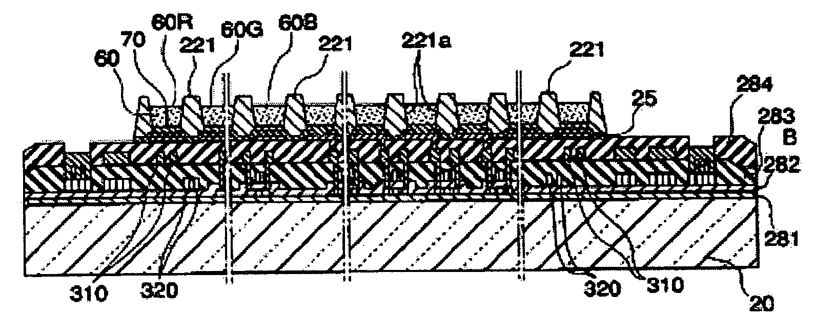
[0044] Hereinafter, embodiments of the electro-optical device, the method of producing the same, and the electronic apparatus of the present invention will be described with reference to the drawings.

[0045] As the electro-optical device, an EL display device using a field light-emissive substance, especially, an organic electroluminescence (EL) material will be described.

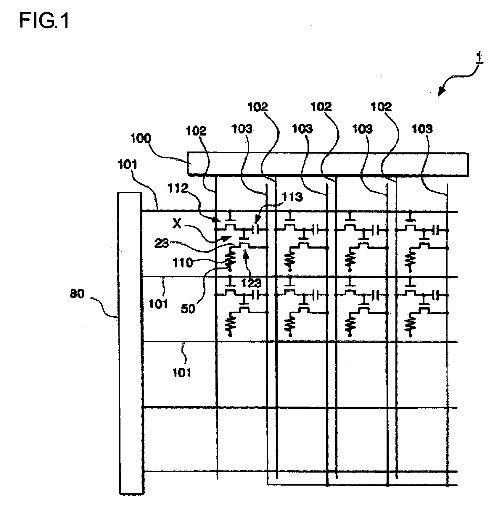
[0046]FIG. 1 shows the wiring configuration of an EL display device 1. The EL display device 1 is an active matrix type EL display device containing thin film transistors (hereinafter, abbreviated to TFT) as switching elements.

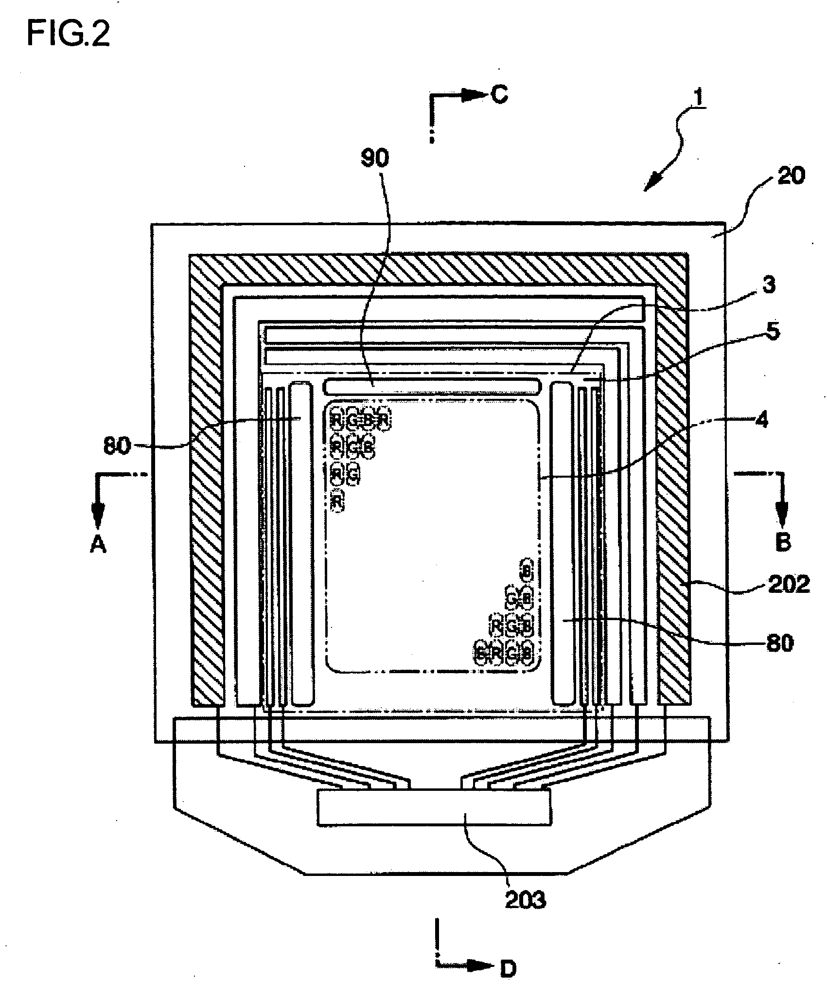
[0047] Referring to the wiring-configuration of the EL display device (electro-optical device) 1, a plurality of scanning lines 101, a plurality of signal lines 102 extended in such a direction as to intersect the respective scanning lines 101 at a right angle, and a plurality of power-supply lines 103 which are extended in parallel to the signal lines 102 are arranged. Moreover, pixel regi...


PUM


Abstract

To provide an electro-optical device in which the fluidity of a material for forming the underlying layer of a gas barrier layer is controlled, and the volume-change of the underlying layer is suppressed, so that stress-concentration on the gas barrier layer is relaxed, and to provide a method of producing the same and an electronic apparatus. In an electro-optical device 1 having, on a substrate 200, a plurality of first electrodes 23, a bank structure 221 having a plurality of openings 221 a positioned correspondingly to the formed first electrodes 23, electro-optical layers 60 arranged in the respective openings, and a second electrode 50 covering the bank structure 221 and the electro-optical layers 60, the device 1 includes a buffer layer 210 formed so as to cover the second electrode 50 and have a substantially flat upper surface, and a gas barrier layer 30 covering the buffer layer 210.

Description

BACKGROUND OF THE INVENTION [0001] 1. Field of Invention [0002] The present invention relates to an electro-optical device, a manufacturing method of the same, and an electronic apparatus equipped with the electro-optical device. [0003] 2. Description of Related Art [0004] It has been one of the subjects in the field of electro-optical devices to enhance the durability of the devices against oxygen, water, and so forth. For example, in organic electroluminescence (hereinafter, abbreviated to organic EL) display devices, which are examples of the electro-optical devices, electro-optical materials (organic EL materials, hole-injection materials, electron-injection materials, or the like) for forming light-emitting layers (electro-optical layers) are deteriorated due to oxygen, water, or the like, and the conductivity of cathodes are reduced due to oxygen, water or the like, and thus, non-light-emitting regions called dark spots are formed. Therefore, problems occur in that the service...

Claims


Application Information

Patent Timeline
IPC IPC(8): G02F1/035H05B33/04G09F9/30H01L27/32H01L51/50H01L51/52H05B33/00H05B33/10H05B33/14H05B33/22
CPCB82Y20/00B82Y30/00H01L27/3244Y10S385/901H01L51/5237H01L2251/5369H01L27/3295H10K59/122H10K59/12H10K50/841H10K50/844H10K2102/331H05B33/04H05B33/10H05B33/22
Inventor HAYASHI, KENJINOZAWA, RYOICHI
Owner INTELLECTUAL KEYSTONE TECH LLC
Why Eureka
Try Eureka