Light emitting device and method of manufacturing the same

a technology of light emitting device and manufacturing method, which is applied in the direction of semiconductor/solid-state device manufacturing, semiconductor/conductor device manufacturing, electrical apparatus, etc., can solve the problems of narrow color tone range and light absorption, and achieve the effect of heat release and high light extraction efficiency

Active Publication Date: 2014-10-02
NICHIA CORP
View PDF20 Cites 25 Cited by
  • Summary
  • Abstract
  • Description
  • Claims
  • Application Information

AI Technical Summary

Benefits of technology

[0014]Alight emitting device according to the disclosure can provi

Problems solved by technology

Light emitting diodes in various color tones are required according to recent applications, and moreover, the range of color tone is very narrowly limited.
However, a disadvantaged resin package type light emitting device which is inte

Method used


Image

  • Light emitting device and method of manufacturing the same
  • Light emitting device and method of manufacturing the same
  • Light emitting device and method of manufacturing the same

Examples


example 1

Illustrative Example 1

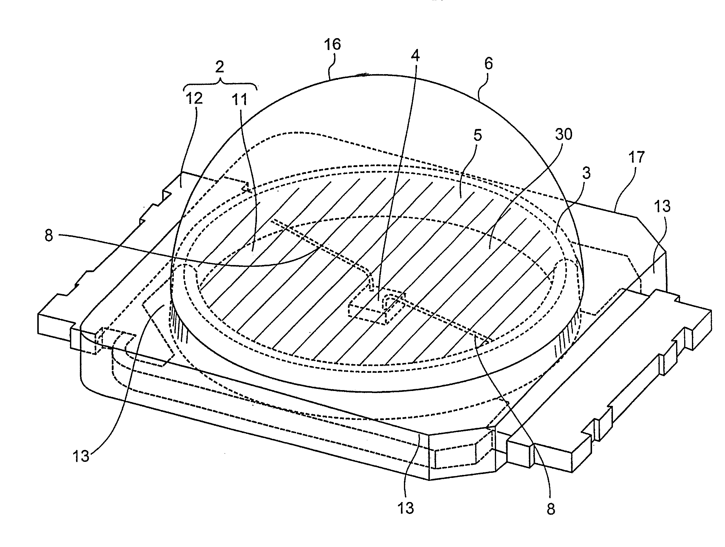
[0122]FIG. 9 shows an example light emitting device 1 having one light emitting element 4 and a molded resin 13 arranged between the cathode 11 and the anode 12 which constitute the lead frame 2. The lead frame 2 has a cathode 11 and the anode 12 each having a shape as shown in FIG. 4. The cathode 11 is formed larger than the anode 12 and the light emitting element 4 is mounted on the cathode 11. The lead frame 2 is made of a clad material which is a stacked layer of an alloy of Fe and Cu, an Invar (registered trademark, an alloy made of iron and 36% nickel), and an alloy of Fe and Cu. Then, Ni, Pd, and Au may be plated in this order from the bottom on the surfaces of the lead frame 2. Further, in order to increase the reflectance of the light emitting portion of the lead frame 2, a plating of Ag may be applied on the Au.

[0123]First, as shown in example FIG. 5, the molded resin 13 is disposed between the cathode 11 and the anode 12, and around the cathode 11 an...

example 2

Illustrative Example 2

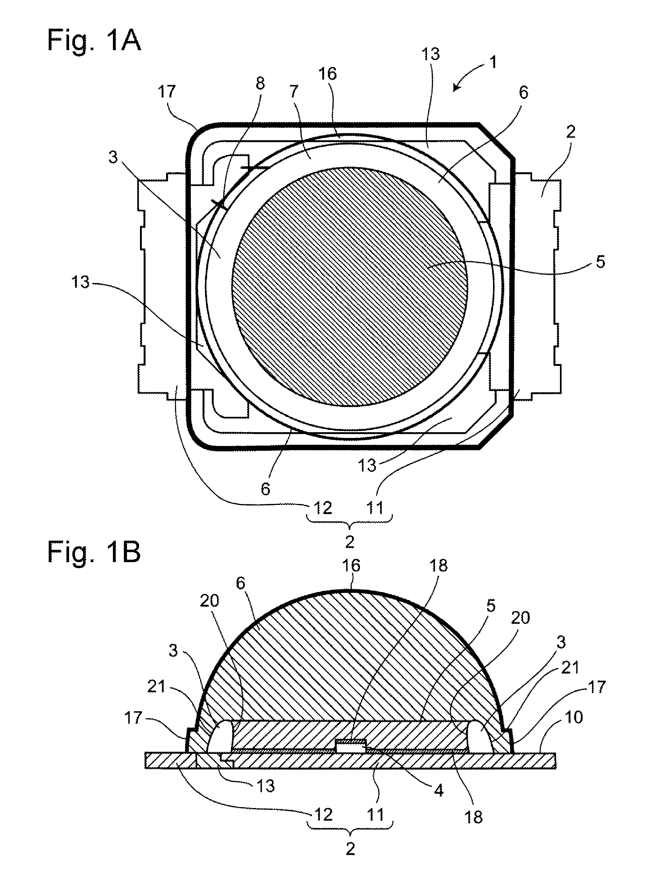
[0129]FIG. 14 shows an example embodiment of a light emitting device 1 having one light emitting element 4, and a molded resin 13 is not arranged between the cathode 11 and the anode 12. The light emitting device according to Illustrative Example 2 has a similar configuration as in Illustrative Example 1, except that in Illustrative Example 1, the molded member 13 is arranged but in Illustrative Example 2, the molded resin 13 is not arranged.

[0130]The cathode 11 and the anode 12 each having a shape as shown in FIG. 10 may be prepared. Then, without forming the molded resin 13 between the cathode 11 and the anode 12, one light emitting element may be mounted on the cathode 11. After the above, the light emitting device may be manufactured in a similar manner as in Illustrative Example 1. In the light emitting device 1 according to Illustrative Example 2, the molded resin 13 is not provided and the resin frame 3 is formed only on the cathode 11, so that as descri...

example 3

Illustrative Example 3

[0131]FIG. 15 shows an example embodiment of a light emitting device 1 having, for example, nine light emitting elements 4 and the molded resin 13 is arranged between the cathode 11 and the anode 12. The light emitting device according to Illustrative Example 3 has a similar configuration as in Illustrative Example 1, except that in Illustrative Example 1, one light emitting element 4 is mounted, but in Illustrative Example 3, nine light emitting elements 4 are mounted in a matrix shape. Implementations of the invention are not limited to such numbers of light emitting elements, i.e., any number of light emitting elements may be included.

[0132]The cathode 11 and the anode 12 each having a shape as shown in FIG. 4 may be prepared, and in a similar manner as in Illustrative Example 1, the molded resin 13 may be formed between the cathode 11 and the anode 12. Then, nine light emitting elements 4 are disposed in a matrix shape, and as shown in FIG. 15, using the bo...


PUM


Abstract

Provided is a light emitting device with improved light extracting efficiency and further higher heat releasing performance. A light emitting device includes a planar lead frame having a first lead and a second lead, and includes a light emitting element mounted on the first lead, a resin frame surrounding a periphery of the light emitting element, a first sealing resin filled in the inner side of the resin frame and sealing the light emitting element, and a second sealing resin covering the resin frame and the first sealing resin. Lower end of inner surface of the resin frame is arranged only on the first lead, and at an outside of the resin frame, and the second resin member covers at least a part of the first lead and the second lead. Of the back-surface of the first lead, a region directly under the blight emitting element is exposed.

Description

CROSS-REFERENCE TO RELATED APPLICATION[0001]This application claims priority to Japanese Patent Application No. 2013-073661, filed on Mar. 29, 2013, and No. 2014-059728, filed on Mar. 24, 2014. The entire disclosure of Japanese Patent Application No. 2013-073661 and No. 2014-059728 are hereby incorporated herein by reference.BACKGROUND[0002]1. Technical Field[0003]The present disclosure relates to a light emitting device applicable, for example, to purposes such as an indicator, a lighting luminaire, a display, and a backlight light source for liquid crystal display.[0004]2. Background Art[0005]Light emitting devices using light emitting elements such as light emitting diodes or laser diodes are employed in various fields such as general lighting such as in-door lighting, on-vehicle lighting, and backlight for liquid crystal displays. Requirements for higher performance in those light emitting devices are growing daily, and light emitting diodes of further higher output (higher lumi...

Claims


Application Information

Patent Timeline
IPC IPC(8): H01L33/54H01L33/58H01L33/50H01L33/62
CPCH01L33/54H01L33/505H01L33/58H01L33/62H01L33/52H01L33/486H01L2224/45144H01L2224/48139H01L2224/48137H01L2224/48091H01L2224/48247H01L2933/005H01L2924/00014H01L2924/00H01L33/507H01L33/56H01L2933/0033H01L2933/0041H01L2933/0066H01L33/46
Inventor UKAWA, HIROAKI
Owner NICHIA CORP
Why Eureka
Try Eureka