Recessed-gate transistor device having a dielectric layer with multi thicknesses and method of making the same

a transistor and dielectric layer technology, applied in the direction of transistors, semiconductor devices, electrical appliances, etc., can solve the problems of reducing the speed of transferring data, deteriorating the reliability of the device, increasing the integration of the semiconductor device and the operating performance, etc., to achieve the effect of improving the operating performance and increasing the landing area

Active Publication Date: 2009-05-07
NAN YA TECH
View PDF6 Cites 59 Cited by
  • Summary
  • Abstract
  • Description
  • Claims
  • Application Information

AI Technical Summary

Benefits of technology

[0014]It is one object of this invention to provide a recessed-gate MOS transistor with a gate dielectric layer with multi thicknesses so as to solve the problem of current leakage and improve the operating performance. Besides, the landing area can be increased.

Problems solved by technology

Consequently, a short channel effect may occur, resulting in problems in increasing the integration of the semiconductor devices and the operating performance.
These methods, however, may deteriorate the reliability of the devices and decrease the speed of transferring data.
Additionally, as the device is scaled down, the landing area, shown by A1, will be too small and lead to the fabricating problems.
These problems may deteriorate the operating performance of the devices.

Method used


Image

  • Recessed-gate transistor device having a dielectric layer with multi thicknesses and method of making the same
  • Recessed-gate transistor device having a dielectric layer with multi thicknesses and method of making the same
  • Recessed-gate transistor device having a dielectric layer with multi thicknesses and method of making the same

Examples


Embodiment Construction

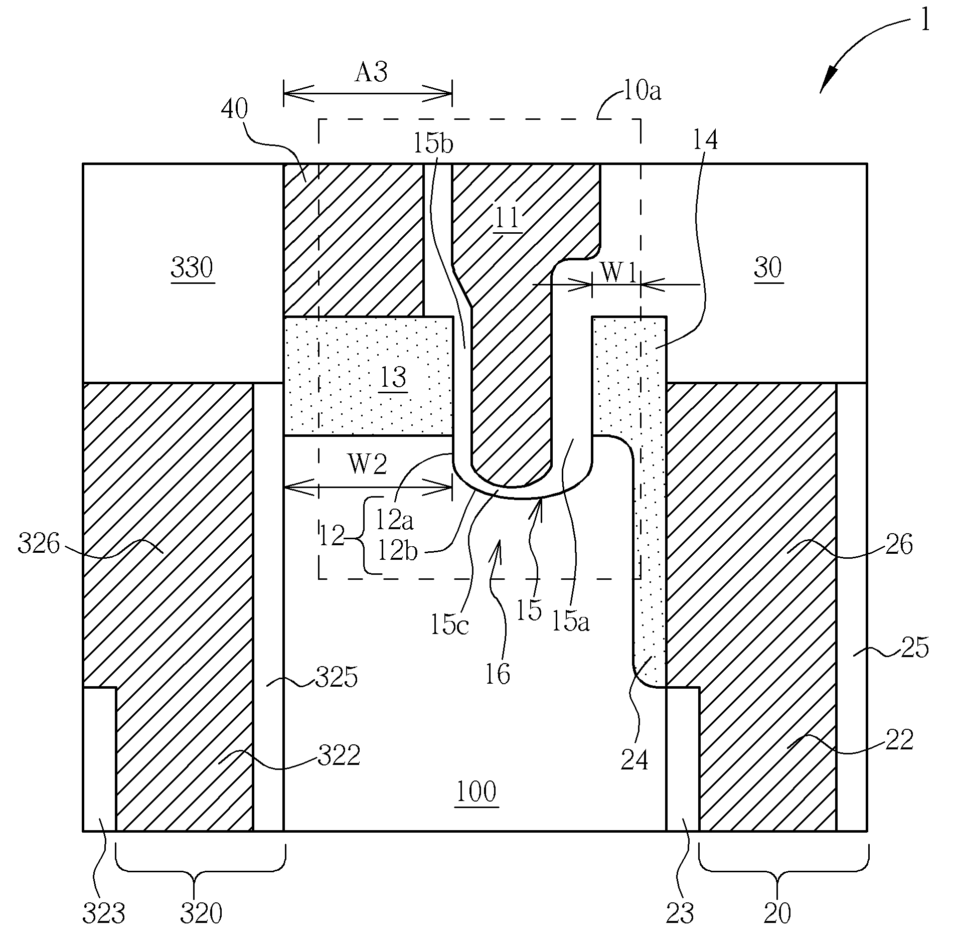
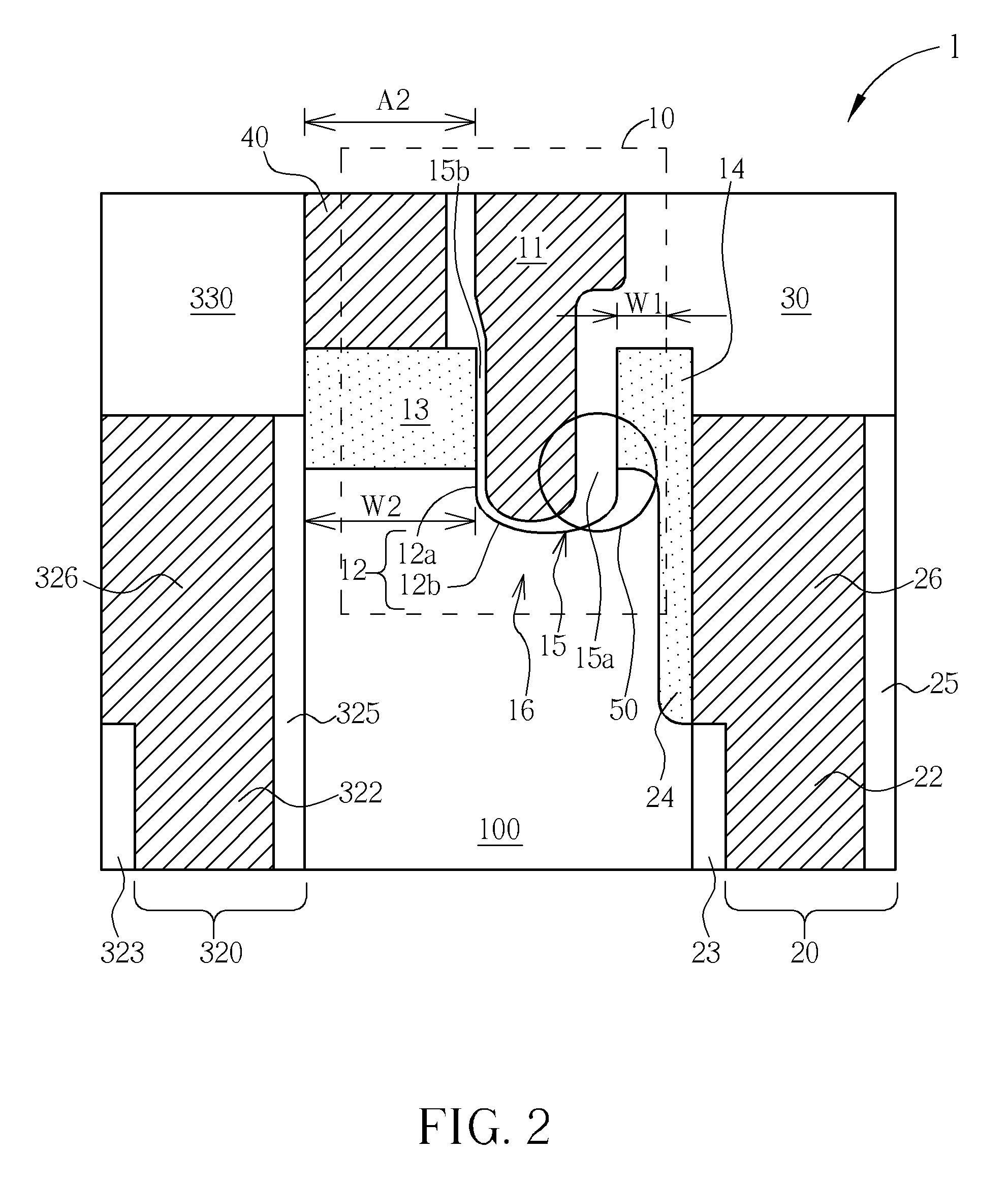
[0024]FIG. 2 is a schematic sectional view showing the recessed-gate MOS transistor device according to this invention. As shown in FIG. 2, a recessed-gate MOS transistor device 10 is positioned in a deep trench capacitor DRAM array 1. Such device 10 is also called a recess channel array transistor device (RCAT). The recessed-gate MOS transistor device 10 and a deep trench capacitor structure 20 that is adjacent to the recessed-gate MOS transistor device 10 constitute a DRAM cell. Besides, another deep trench capacitor 320, which is adjacent to the recessed-gate MOS transistor device 10 and belong to another DRAM cell, is also demonstrated.

[0025]According to a preferred embodiment of the present invention, the recessed-gate MOS transistor device 10 includes a recessed gate electrode 11, a source region 13, a drain region 14, and a gate dielectric layer 15. The source region 13 has a second width W2 and the drain region 14 has a first width W1. The recessed gate electrode 11 is embed...


PUM


Abstract

A recessed-gate transistor device includes a gate electrode embedded in a gate trench formed in a semiconductor substrate, wherein the gate trench includes a vertical sidewall and a U-shaped bottom. A source region is provided at one side of the gate trench within the semiconductor substrate. A drain region is provided at the other side thereof. An asymmetric gate dielectric layer is formed between the gate electrode and the semiconductor substrate. The asymmetric gate dielectric layer has a first thickness between the gate electrode and the drain region and a second thickness between the gate electrode and the source region, wherein the first thickness is thicker than the second thickness.

Description

BACKGROUND OF THE INVENTION[0001]1. Field of the Invention[0002]The present invention relates to structures of a semiconductor device, and methods of making the same, and more particularly, to a recessed-gate transistor device having a dielectric layer with multi thicknesses.[0003]2. Description of the Prior Art[0004]As the size of semiconductor devices shrinks, the gate channel length decreases correspondingly. Consequently, a short channel effect may occur, resulting in problems in increasing the integration of the semiconductor devices and the operating performance.[0005]The conventional method of solving the short channel effect includes decreasing the thickness of the gate oxide layer or increasing concentration of the dopants. These methods, however, may deteriorate the reliability of the devices and decrease the speed of transferring data.[0006]To solve the above-mentioned problems, a recessed-gate transistor design or an extended U-shape device (EUD) is used in the semicondu...

Claims


Application Information

Patent Timeline
Patent Type & Authority Applications(United States)
IPC IPC(8): H01L21/265H01L29/78H01L27/108
CPCH01L21/26506H01L21/26586H01L29/66621H01L29/4236H01L29/42368H01L27/10876H10B12/053
Inventor WANG, JER-CHYIWU, TIEH-CHIANGLEE, CHUNG-YUANLIN, JENG-PING
Owner NAN YA TECH
Why Eureka
Try Eureka