Plasma display panel and method of producing the same

Inactive Publication Date: 2009-05-07
PANASONIC CORP
View PDF3 Cites 4 Cited by
  • Summary
  • Abstract
  • Description
  • Claims
  • Application Information

AI Technical Summary

Benefits of technology

[0014]In view of the above problems, it is an object of the present invention to provide a highly reliable plasma display panel that is provided with a dielectric layer having a high withstand voltage and that prevents not only the dielectric layer and the glass substrate from yellowing but also dielectric breakdown from occurring. It is also an object of the present invention to provide a method of producing the same.
[0029]In the plasma display panel obtained by the present invention, the first glass that is contained in the first dielectric layer contains at least one selected from MoO3 and WO3. Accordingly, even if Ag or Cu that commonly is used as an electrode material ionizes and then diffuses in the dielectric layer, it produces a stable compound together with MoO3 or WO3, which prevents Ag or Cu from aggregating and becoming colloidal. This prevents the dielectric layer from yellowing due to the colloidal form of Ag or Cu. Similarly, in the case where the electrodes are formed on a glass substrate, Ag or Cu that has diffused in the glass substrate produces a stable compound together with MoO3 or WO3. Accordingly, the glass substrate also can be prevented from yellowing due to the colloidal form of Ag or Cu. Furthermore, the plasma display panel according to the present invention can prevent the occurrence of not only yellowing but also other harmful effects that accompany the production of Ag or Cu colloids, for example, a decrease in withstand voltage of the dielectric layer and a deterioration in luminance of the PDP.
[0031]Moreover, in the plasma display panel obtained by the present invention, the first glass can contain the suitable components as shown above. The first glass further can contain at least one selected from the group consisting of Li2O, Na2O and K2O. This makes it possible not only to prevent the dielectric breakdown from occurring and the dielectric layer and the glass substrate from yellowing due to the colloidal form of Ag or Cu, but also to lower or adjust the softening point of the glass, thanks to at least one selected from the group consisting of Li2O, Na2O and K2O. Moreover, the addition of these components (Li2O, Na2O and K2O) having a function of lowering the softening point allows the content of Bi2O3, which is a component having a function of increasing the relative dielectric constant as well as the same function as the components (Li2O, Na2O and K2O), to be reduced. Accordingly, the relative dielectric constant of the dielectric can be lowered or adjusted.

Problems solved by technology

Accordingly, the dielectric layer may be colored by carbon-containing impurities that remain therein, which may cause a deterioration in luminance.
Since such yellowed glass absorbs light with a wavelength of 400 nm, a PDP produced using the glass has inferior blue luminance or inferior chromaticity.
Hence, yellowing is a problem, especially in the front panel.
Furthermore, since Ag colloids and Cu colloids have conductivity, they lower the withstand voltage of the dielectric layer.
In addition, since Ag and Cu colloids deposit as colloidal particles that are far larger than ions, they reflect the light that passes through the dielectric layer and thereby cause the deterioration in luminance of the PDP.

Method used


Image

  • Plasma display panel and method of producing the same
  • Plasma display panel and method of producing the same
  • Plasma display panel and method of producing the same

Examples


examples

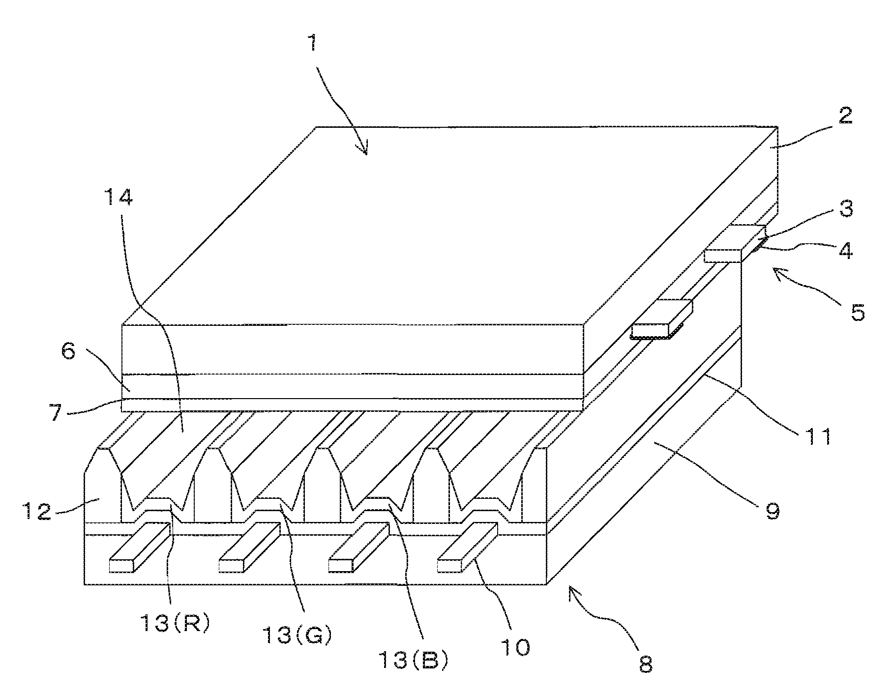
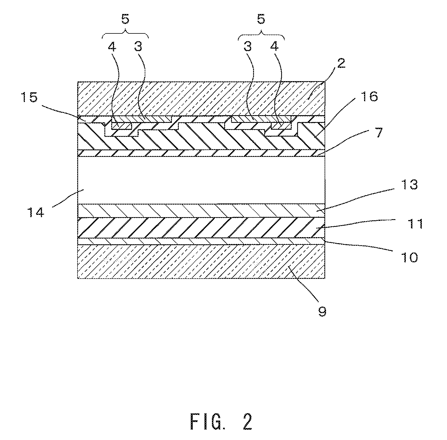
[0137]Hereinafter, the present invention is described further in detail using examples.

[0138]Glass samples to be used for the dielectric layers of the PDP according to the present invention were produced. Tables 1 to 7 show the compositions of the glass samples to be used for dielectric layers of the PDP according to the present invention. Tables 8 to 11 show the compositions of the glass samples that were produced in order to examine the effect of decreasing the degree of yellowing through the addition of MoO3 and WO3 in the present invention. Glass samples shown in Tables 12 and 13 are the samples that can be used to describe the preferred contents of components in respective glass compositions to be used for the PDP according to the present invention. In the tables, “SiO2” is indicated as “SiO2”, for example.

TABLE 1GlassNo.Composition12345678910SiO215.009.701.0014.909.3012.001.601.50B2O327.3029.5030.9010.0015.0050.0024.2030.6023.4026.90ZnO27.0026.8026.0033.6035.7026.0015.0031.803...


PUM

PropertyMeasurementUnit
Temperatureaaaaaaaaaa
Currentaaaaaaaaaa

Abstract

A plasma display panel of the present invention includes a display electrode (5) and an address electrode (10) that cross each other. At least one selected from the display electrode (5) and the address electrode (10) is covered with a first dielectric layer (6) containing first glass. The first glass contains Bi2O3, and the electrode that is covered with the first dielectric layer (6) contains at least one selected from the group consisting of silver and copper. The first glass further contains 0 to 4 wt % of MoO3 and 0 to 4 wt % of WO3, and the total of the contents of MoO3 and WO3 in the first glass is in a range of 0.1 to 8 wt %.

Description

TECHNICAL FIELD[0001]The present invention relates to a plasma display panel and a method of producing the same.BACKGROUND ART[0002]In recent years, flat panel displays, such as plasma display panels (hereinafter also referred to as “PDPs”), FEDs, and liquid crystal displays, have been gaining attention as displays that can achieve reductions in thickness and weight.[0003]These flat panel displays each are provided with a front panel and a back panel, each of which includes a glass substrate and components disposed thereon. The front panel and the back panel are arranged to oppose each other, and the peripheries thereof are sealed.[0004]As described above, a PDP has a configuration in which the front panel and the back panel are arranged to oppose each other and the peripheries thereof are sealed with sealing glass. The front panel includes: a front glass substrate; stripe-like display electrodes that are formed on the surface of the front glass substrate; and a dielectric layer and...

Claims


Application Information

Patent Timeline
IPC IPC(8): H01J17/49H01J9/24C03C8/04H01J9/02H01J11/12H01J11/22H01J11/24H01J11/26H01J11/34H01J11/38
CPCC03C8/04C03C12/00C03C17/04C03C17/36H01J11/38C03C2217/94C03C2217/948H01J9/02H01J11/12C03C17/3671C03C3/066C03C3/068C03C3/064
Inventor HASEGAWA, SHINYAINOUE, OSAMUKAWASE, AKIRANAKADA, YASUHIKOYOKOTA, KAZUHIROKOSHIZUKA, TSUTOMUTOYODA, SEIJI
Owner PANASONIC CORP
Why Eureka
Try Eureka