Display apparatus, display-apparatus driving method and electronic instrument

a technology of display apparatus and driving method, which is applied in the direction of electrical apparatus, electric discharge tubes, instruments, etc., can solve the problems of excessive mobility correction process and undesirable gradual decrease of light emission current of organic el devices, so as to prevent the operating point of the mobility correction process from changing, prevent the effect of light emission current from decreasing and neutralize the shi

Active Publication Date: 2009-05-07
JOLED INC
View PDF2 Cites 14 Cited by
  • Summary
  • Abstract
  • Description
  • Claims
  • Application Information

AI Technical Summary

Benefits of technology

[0040]In a display apparatus having a configuration for sequentially carrying out the threshold-voltage correction process and the mobility correction process in a no-light emission period of the electro optical device as described above and an electronic instrument employing such a display apparatus, when a current is not flowing through the device driving transistor in a no-light emission period of the electro optical device, the pixel driving section deliberately applies a positive bias voltage to the gate electrode of the signal writing transistor in order to shift the Vth characteristic of the signal writing transistor to an enhancement side. By shifting the Vth characteristic of the signal writing transistor to an enhancement side in a no-light emission period of the electro optical device as described above, it is possible to neutralize a shift caused by a negative bias voltage applied to the gate electrode of the signal writing transistor during a light emission period leading ahead of the no-light emission period as a shift of the Vth characteristic to a depletion side. As a result, it is possible to prevent the operating point of the mobility correction process from changing.
[0041]In accordance with the embodiments of the present invention, when a current is not flowing through the device driving transistor in a no-light emission period of the electro optical device, the pixel driving section applies a positive bias voltage to the gate electrode of the signal writing transistor in order to shift the Vth characteristic of the signal writing transistor to an enhancement side. It is thus possible to neutralize a shift caused by a negative bias voltage applied to the gate electrode of the signal writing transistor during a light emission period of the electro optical device when a current is flowing through the device driving transistor as a shift of the Vth characteristic to a depletion side. As a result, a light emission current can be prevented from decreasing due to a shift occurring in the light emission period leading ahead of the no-light emission period as a shift of the Vth characteristic to the depletion side.

Problems solved by technology

Thus, the mobility correction process is carried out excessively.
As a result, a light emission current of the organic EL device undesirably decreases in a gradual manner.

Method used


Image

  • Display apparatus, display-apparatus driving method and electronic instrument
  • Display apparatus, display-apparatus driving method and electronic instrument
  • Display apparatus, display-apparatus driving method and electronic instrument

Examples


first embodiment

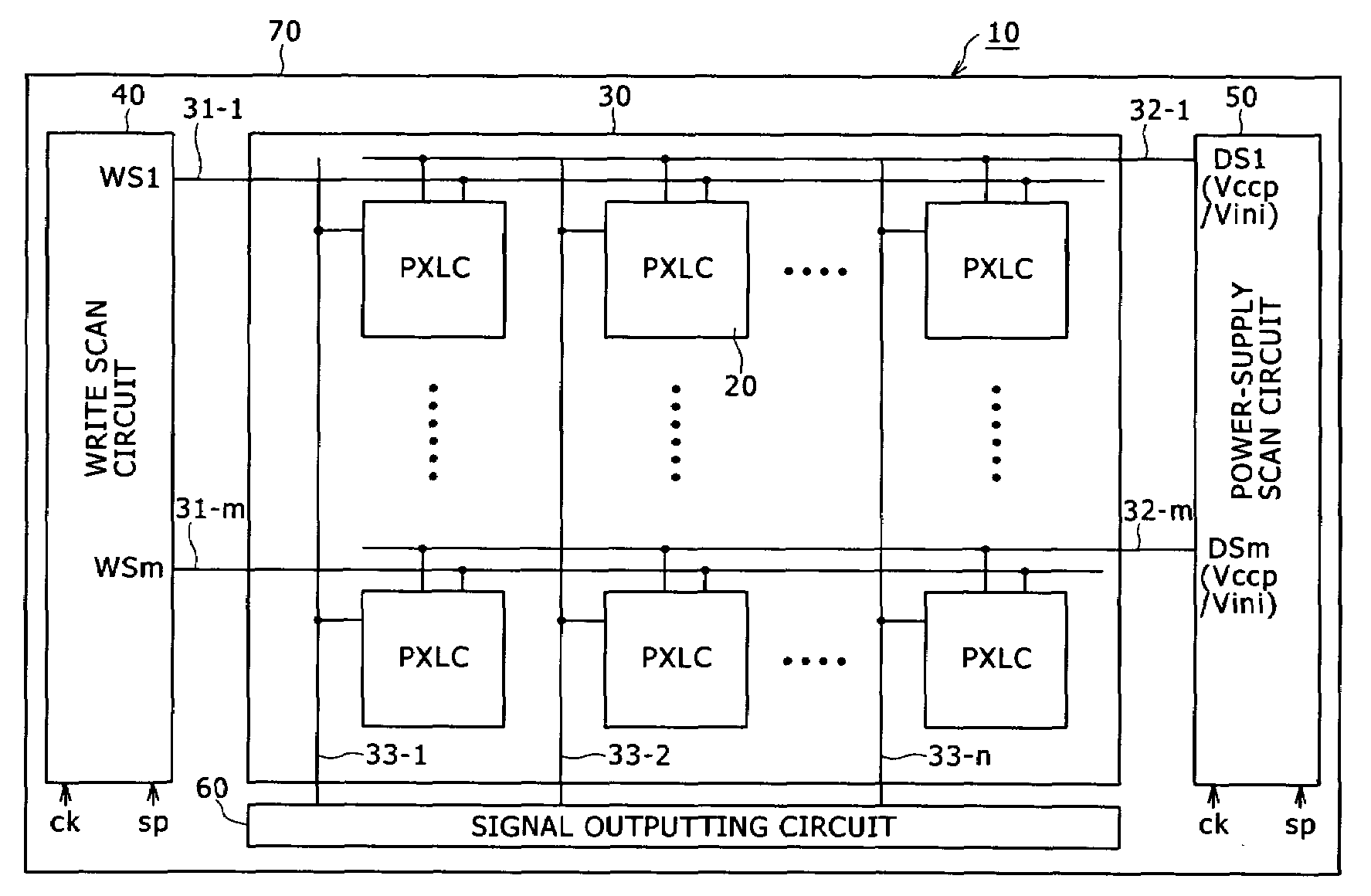
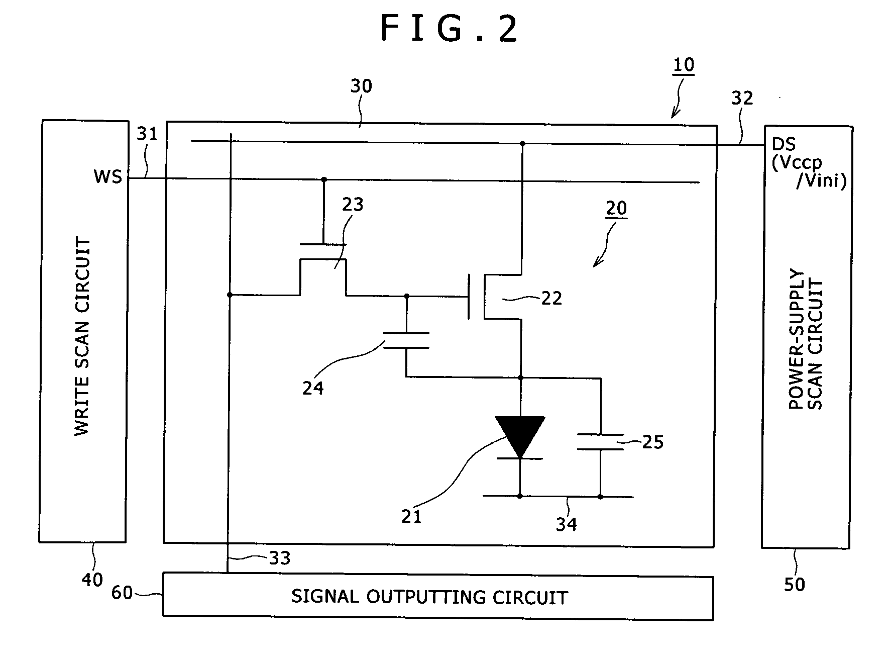
[0169]FIG. 14 is a timing / waveform diagram referred to in description of circuit operations which are carried out in accordance with a driving method provided by a first embodiment.

[0170]As shown in the timing / waveform diagram of FIG. 14, at a time t1, a new frame referred to as the present frame arrives. Then, at a time t2, an electric potential Vg applied to the gate electrode of the device driving transistor 22 is initialized at the reference electric potential Vofs whereas an electric potential Vs applied to the source electrode of the device driving transistor 22 is initialized at the low electric potential Vini. After the initialization processes, during a period between times t3 and t4, a threshold-voltage correction process is carried out and, during a period between times t6 and t7, a signal writing operation to store the video-signal voltage Vsig into the signal storage capacitor 24 as well as a mobility correction process are carried out. The processing series composed of...

second embodiment

[0175]FIG. 15 is a timing / waveform diagram referred to in description of circuit operations which are carried out in accordance with a driving method provided by a second embodiment.

[0176]In the case of the first embodiment, the positive bias voltage is applied to the gate electrode of the signal writing transistor 23 by setting the electric potential WS in an active state intermittently during a plurality of 1H periods in such a way that the electric potential WS is put in the active state once during each of the 1H periods while an electric potential appearing on the signal line 33 is being set at the reference electric potential Vofs. In the case of the second embodiment, on the other hand, a positive bias voltage is also applied to the gate electrode of the signal writing transistor 23 or, to put it concretely, the electric potential WS is set at an active level (or a high level) and applied to the gate electrode of the signal writing transistor 23 but the positive bias voltage ...

application examples

[0195]The display apparatus according to the present invention described above is typically employed in a variety of electronic instruments shown in diagrams of FIGS. 16 to 20G as instruments used in all fields. Examples of the electronic instruments are a digital camera, a laptop personal computer, a portable terminal such as a cellular phone and a video camera. In each of these electronic instruments, the display apparatus is used for displaying a video signal supplied thereto or generated therein as an image or a video.

[0196]By employing the display apparatus according to the present invention in a variety of electronic instruments used in all fields as the display unit of each of the instruments, as is obvious from the embodiments described previously, the display apparatus provided by embodiments of the present invention is capable of preventing the light emission current of the organic EL device 21 from decreasing because of the fact that the Vth characteristic is shifted to t...


PUM


Abstract

Disclosed herein is a display apparatus including: a pixel array section including pixel circuits each having an electro optical device, a signal writing transistor, a signal storage capacitor, and a device driving transistor; and a pixel driving section, wherein: in a no-light emission period, the pixel driving section carries out a threshold-voltage correction process by changing an electric potential appearing on an electrode of the device driving transistor close to the electro optical device toward an electric potential obtained by subtracting the threshold voltage of the device driving transistor from the initialization electric potential of the gate electrode of the device driving transistor and a mobility correction process of negatively feeding a current flowing through the device driving transistor back to the gate electrode of the device driving transistor; and when a current is not flowing through the device driving transistor, the pixel driving section applies a positive bias voltage to the gate electrode of the signal writing transistor.

Description

CROSS REFERENCES TO RELATED APPLICATIONS[0001]The present invention contains subject matter related to Japanese Patent Application JP 2007-289309 filed in the Japan Patent Office on Nov. 7, 2007, the entire contents of which being incorporated herein by reference.BACKGROUND OF THE INVENTION[0002]1. Field of the Invention[0003]In general, the present invention relates to a display apparatus, a display-apparatus driving method and an electronic instrument. In particular, the present invention relates to a display apparatus having the type of a flat panel having pixels laid out two-dimensionally to form a matrix as pixels each including an electro optical device and relates to a method for driving the display apparatus as well as an electronic instrument employing the display apparatus.[0004]2. Description of the Related Art[0005]In recent years, in the field of display apparatus for displaying images, a display apparatus having the type of a flat panel having pixels laid out two-dimen...

Claims


Application Information

Patent Timeline
Patent Type & Authority Applications(United States)
IPC IPC(8): G09G3/30
CPCG09G3/3233G09G2300/0852G09G2300/0819H01J37/2955H10K59/35
Inventor YAMASHITA, JUNICHIYAMAMOTO, TETSUROUCHINO, KATSUHIDE
Owner JOLED INC
Why Eureka
Try Eureka