
Semiconductor device including main substrate and sub substrates and fabrication method of the same

Inactive Publication Date: 2009-05-14
ONKYO KK
View PDF2 Cites 16 Cited by
  • Summary
  • Abstract
  • Description
  • Claims
  • Application Information

AI Technical Summary

Benefits of technology

[0009]With this structure, the sub-substrate heatsinks and the main-substrate heatsink, which are mounted for releasing heat, are secured to each other, so that there is a predetermined positional relationship between the sub substrates and the main substrate. Therefore, this can eliminate the necessity of using dedicated jigs or additional dedicated securing members, in order to secure the sub substrates and the main substrate to each other such that there is a predetermined positional relationship between the sub substrates and the main substrate. This can reduce the number of assembling processes, in comparison with cases of using dedicated jigs as described above. Also, this can reduce the number of assembling processes and also can reduce the material cost, in comparison with cases of using additional dedicated securing members as described above.

Problems solved by technology

In cases of assembling using dedicated jigs, there is induced inconvenience of increase of the number of assembling processes.
Further, it is also possible to employ a method which uses additional securing members, but such a method induces the problem of increase of assembling processes due to the increase of the number of components and, further, induces the problem of increase of the material cost by an amount corresponding to the additional components.

Method used


Image

  • Semiconductor device including main substrate and sub substrates and fabrication method of the same
  • Semiconductor device including main substrate and sub substrates and fabrication method of the same
  • Semiconductor device including main substrate and sub substrates and fabrication method of the same

Examples


first embodiment

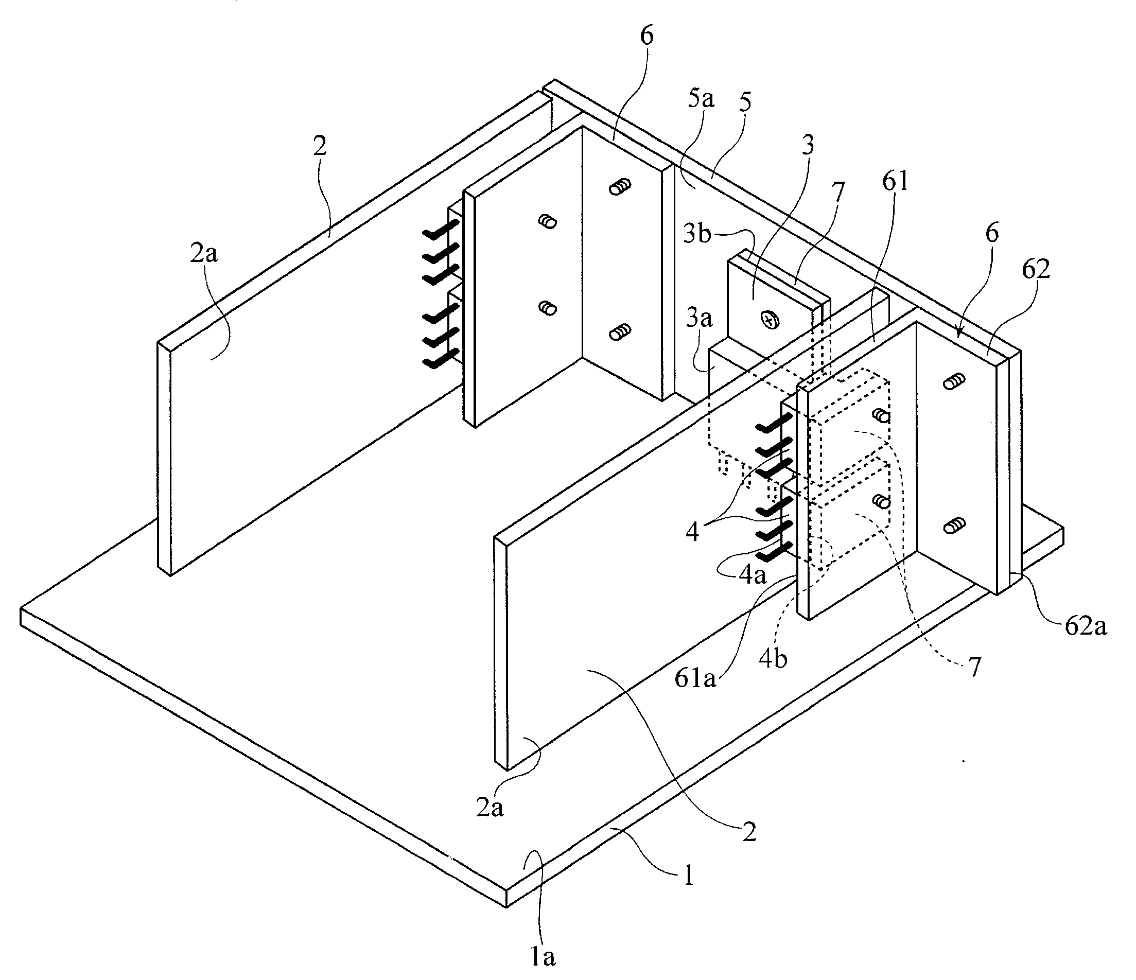
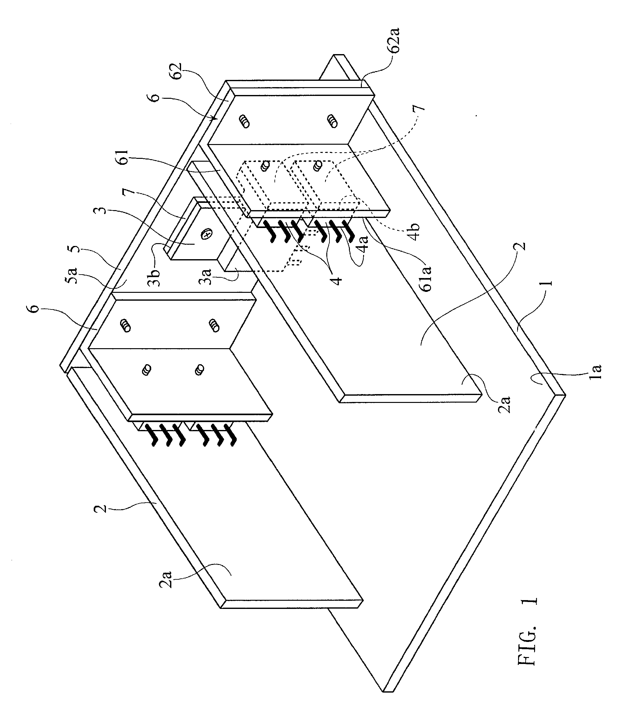
[0034]FIG. 1 is a view showing an internal structure of a semiconductor device according to the present invention. In FIG. 1, components which are not required to be described are not illustrated.

[0035]The semiconductor device includes a main substrate 1, sub substrates 2, a power-supply rectification diode 3, power transistors 4, a main-substrate heatsink 5, sub-substrate heatsinks 6, heat transfer sheets 7, and an outer case which is not illustrated.

[0036]The main substrate 1 is a power-supply substrate, and electronic components constituting a power supply device and electronic components for controlling are mounted on a mounting surface 1a thereof (the surface at the front side in FIG. 1). The respective electronic components are electrically interconnected, through wiring patterns provided on the mounting surface 1a and the back surface of the main substrate 1. In FIG. 1, the wiring patterns and the electronic components other than the power-supply rectification diode 3, which ...

second embodiment

[0061]In the second embodiment, similarly, there is no need for using dedicated jigs or dedicated securing members for securing the sub substrates 2 to the main substrate 1. Further, since the main-substrate heatsink 5′ is secured to the chassis 10 of the outer case, the chassis 10 of the outer case also functions as a heat releasing member. This can efficiently release heat generated from the heat generating devices, such as the power-supply rectification diode 3 and the power transistors 4.

[0062]Further, the method for securing the main-substrate heatsink 5′ to the chassis 10 of the outer case is not limited to the aforementioned method, and a heat transfer sheet 7 can be interposed therebetween or they can be secured to each other through other methods than securing with screws. For example, the main-substrate heatsink 5′ can be directly adhered to the chassis 10 with an adhesive agent with a lower thermal resistance or can be secured to the chassis 10 by soldering or welding. Fu...

third embodiment

[0066]While, in the third embodiment, the main-substrate heatsink 5 and the sub-substrate heatsinks 6′, which have been originally used for releasing heat, are used for securing the sub substrates 2 to the main substrate 1, which therefore eliminates the necessity of using dedicated jigs or dedicated securing members for securing the sub substrates 2 to the main substrate 1. Accordingly, this can reduce the number of assembling processes and also can reduce the material cost.

[0067]Further, in the third embodiment, the other surfaces 6′b of the sub-substrate heatsinks 6 are entirely contacted with the main-substrate heatsink 5, which can offer an advantage of making the efficient of the heat transfer from the sub-substrate heatsinks 6′ to the main-substrate heatsink 5 to be higher than those in the first and second embodiments.

[0068]Further, in the third embodiment, the sub-substrate heatsinks 6′ and the sub substrates 2 are secured to each other only with the respective terminals 4c...


PUM


Abstract

A semiconductor device according to a preferred embodiment of the present invention is a semiconductor device including a main substrate and one or more sub substrates, and the semiconductor device includes first heat generating devices mounted on the sub substrates, sub-substrate heatsinks mounted to the first heat generating devices, and a main-substrate heatsink mounted to the main substrate, wherein the sub-substrate heatsinks and the main-substrate heatsink are secured to each other, such that there is a predetermined positional relationship between the sub substrates and the main substrate.

Description

BACKGROUND OF THE INVENTION[0001]1. Field of the Invention[0002]The present invention relates to a semiconductor device including two or more substrates.[0003]2. Description of the Related Art[0004]Large numbers of electronic components are used in semiconductor devices which have been developed in recent years, in order to realize higher performance. The numbers of substrates for use in mounting such electronic components tend to be increased, although the mounting densities of respective substrates have been increased. On the other hand, there are requirements for reduction of the sizes of semiconductor devices. To cope with these requirements, substrates have been stereoscopically assembled, in order to increase the mounting densities.[0005]In cases where substrates are stereoscopically assembled, it is necessary that, to a substrate forming a base (hereinafter, referred to as a “main substrate”), other substrates (hereinafter, substrates secured to the “main substrate” will be r...

Claims


Application Information

Patent Timeline
IPC IPC(8): H01L23/36H01L21/58
CPCH01L23/4006H01L25/112H01L2023/4056H05K1/0203H05K1/14H05K3/301H05K3/366H01L2924/0002H05K2201/10166H05K2201/10409H05K2201/1056H01L2924/00
Inventor MINAKAWA, ATSUSHISEKIYA, MAMORUUMEZU, NORIO
Owner ONKYO KK
Learn More