Circuit and method for reducing output noise of regulator

a technology of output noise and circuit, applied in the direction of electric variable regulation, process and machine control, instruments, etc., can solve the problem of output voltage vo including unintended noise (voltage drop)

Active Publication Date: 2009-05-14
NXP USA INC
View PDF3 Cites 58 Cited by
  • Summary
  • Abstract
  • Description
  • Claims
  • Application Information

AI Technical Summary

Problems solved by technology

This results in the output voltage VO inc

Method used


Image

  • Circuit and method for reducing output noise of regulator
  • Circuit and method for reducing output noise of regulator
  • Circuit and method for reducing output noise of regulator

Examples


first embodiment

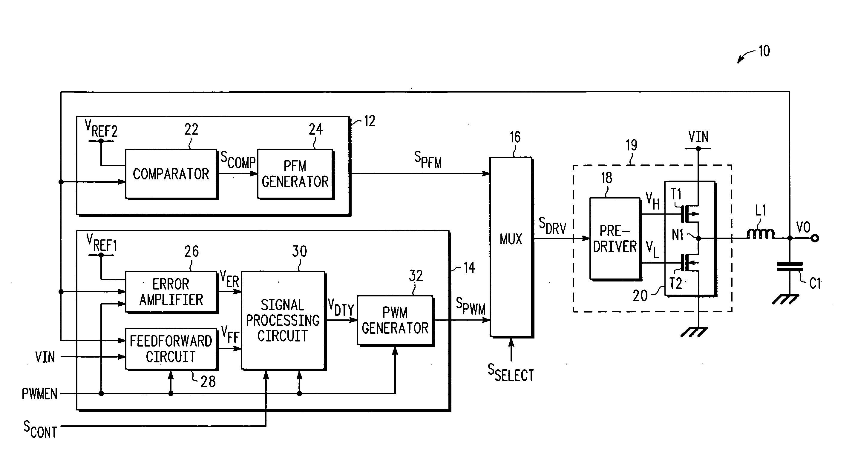
[0051]The mode selection signal SSELECT shifts from the second level to the first level based on the enable signal PWMEN. In the first embodiment, the mode selection signal SSELECT shifts from the second level to the first level when a predetermined time elapses after assertion of the enable signal PWMEN. Thus, the operation mode switches from the PFM mode to the PWM mode when the predetermined time elapses after the PWM circuit 14 is activated. The operation mode switches from the PFM mode to the PWM mode when the duty cycle of the first pulse signal SPWM is stabilized. In other words, the PWM mode is started only after the duty cycle of the first pulse signal SPWM is stabilized. This prevents an unstable drive pulse signal SDRV from being generated when the PWM mode is started.

[0052]The drive pulse signal SDRV, which is output from the multiplexer 16, is provided to the pre-driver 18 of the drive circuit 19. The pre-driver 18 generates the first and second drive signals VH and VL ...

second embodiment

[0074]FIG. 8 is a schematic block circuit diagram of a regulator circuit 60 according to the present invention.

[0075]The regulator circuit 60 of the second embodiment includes a DDC circuit 62 and an LDO circuit 64. The DDC circuit 62 includes a PWM circuit 72, a pre-driver 74, and an output circuit 20. The PWM circuit 72 is formed by either the PWM circuit 14 in FIG. 5 or the PWM circuit 40 in FIG. 6. The pre-driver 74 and the output circuit 20 form a drive circuit of the present invention. The drive circuit operates in the same manner as the drive circuit 19 of FIG. 5.

[0076]In the PWM mode, the PWM circuit 72 receives an output voltage VO1 (VO) via a feedback loop FB1 and controls the duty cycle of a first pulse signal SPWM in accordance with the level of the received output voltage VO1. The pre-driver 74 generates drive signals VH and VL based on the first pulse signal SPWM. Transistors T1 and T2 are driven in a complementary manner based on the drive signals VH and VL. As a resu...


PUM


Abstract

A circuit and a method for reducing output noise when a pulse width modulation mode is started. A pulse width modulation circuit generates a first pulse signal having a duty cycle that is in accordance with an output voltage of a regulator circuit. A drive circuit generates the output voltage from an input voltage in response to the first pulse signal provided from the pulse width modulation circuit. A feed forward circuit controls the pulse width modulation circuit in a manner to generate the first pulse signal having a duty cycle that maintains the output voltage at a desired level before the pulse width modulation circuit provides the first pulse signal to the drive circuit.

Description

BACKGROUND OF THE INVENTION[0001]The present invention relates to a regulator circuit for generating power supply voltage, and more particularly, to a circuit and method for reducing output noise generated when a pulse width modulation (PWM) mode is started.[0002]In the prior art, DDC circuits (DC-DC converters) are known as regulator circuits. A DDC circuit typically includes either a PWM circuit or a pulse frequency modulation (PFM) circuit or includes both PWM and PFM circuits. The PWM circuit adjusts the pulse width of a pulse signal for driving an output transistor in accordance with an output voltage to maintain a constant power supply voltage, which is be supplied to a load. The PFM circuit selectively generates a pulse signal in accordance with the output voltage and adjusts the frequency of the pulse signal. Other examples of regulator circuits include linear regulators that linearly control an output voltage, such as low dropout (LDO) circuits. For example, Japanese Laid-O...

Claims


Application Information

Patent Timeline
IPC IPC(8): G05F1/10G05F1/02
CPCH02M2001/0022H02M3/156H02M1/0022Y10S323/901
Inventor AIURA, MASAMIEGAWA, KANJIMURAKAMI, SHINTAROH
Owner NXP USA INC
Why Eureka
Try Eureka