Method of Forming a Semiconductor Device Having a Strained Silicon Layer on a Silicon-Germanium Layer

a technology of strained silicon and silicon-germanium layer, which is applied in the field of semiconductor devices and semiconductor devices, can solve problems such as deteriorating the electrical characteristics of strained silicon layers

Inactive Publication Date: 2009-05-21
SAMSUNG ELECTRONICS CO LTD
View PDF11 Cites 25 Cited by
  • Summary
  • Abstract
  • Description
  • Claims
  • Application Information

AI Technical Summary

Benefits of technology

[0016]Before forming the SiGe layer, the method may further include forming a Si layer having a higher impurity concentration than the silicon substrate on the silicon substrate.

Problems solved by technology

These threading dislocations in the strained silicon layer may deteriorate the electrical characteristics of the strained silicon layer.

Method used


Image

  • Method of Forming a Semiconductor Device Having a Strained Silicon Layer on a Silicon-Germanium Layer
  • Method of Forming a Semiconductor Device Having a Strained Silicon Layer on a Silicon-Germanium Layer
  • Method of Forming a Semiconductor Device Having a Strained Silicon Layer on a Silicon-Germanium Layer

Examples


experimental examples

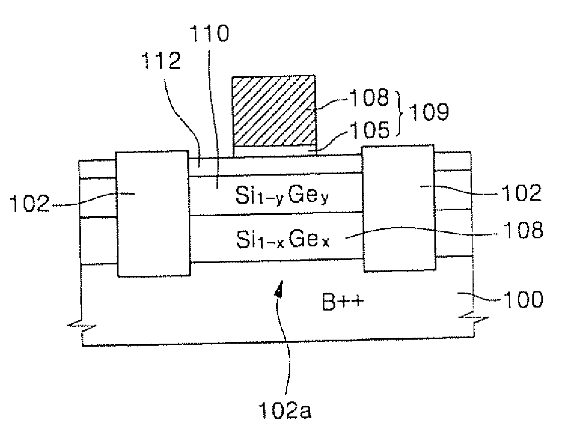
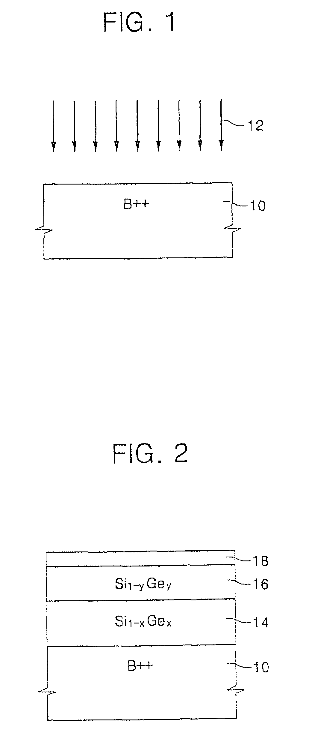
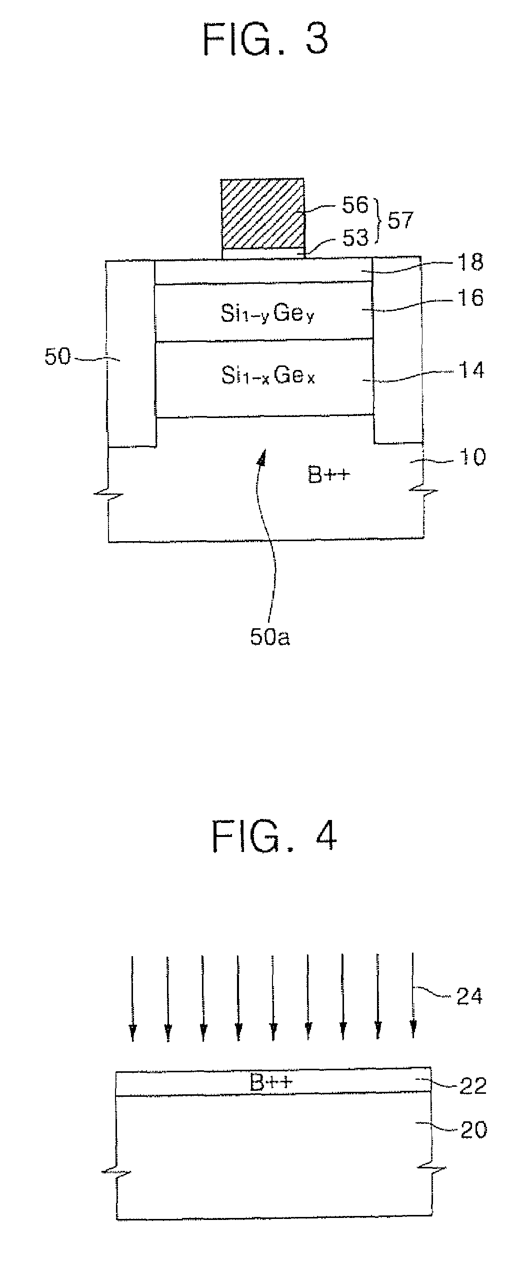
[0058]FIG. 13 is a graph of the dislocation density near the upper surface of a strained silicon layer of a semiconductor structure fabricated in accordance with embodiments of the present invention. In FIG. 13, the x-axis indicates the germanium concentration gradient in a graded SiGe layer of the semiconductor structure, and the y-axis indicates the dislocation density near the surface of the strained silicon layer. Here, the data points represented by a “” (solid circle) show results that were obtained by sequentially forming a graded SiGe layer, a relaxed SiGe layer and a strained silicon layer on a silicon substrate doped with boron at a concentration of about 1019 / cm3 according to exemplary embodiments of the present invention. The data points represented by a “▪” (solid square) show results that were obtained by sequentially forming a graded SiGe layer, a relaxed SiGe layer and a strained silicon layer on a silicon substrate doped with boron at a concentration of about 1015 / ...


PUM

PropertyMeasurementUnit
thicknessaaaaaaaaaa
thicknessaaaaaaaaaa
thicknessaaaaaaaaaa

Abstract

A method of forming a semiconductor device having a strained silicon (Si) layer on a silicon germanium (SiGe) layer is provided. The method includes preparing a silicon substrate. A SiGe layer is formed on the silicon substrate. At least a part of the SiGe layer has a first dislocation density. A strained Si layer having a second dislocation density lower than the first dislocation density is formed on the SiGe layer.

Description

CROSS-REFERENCE TO RELATED APPLICATION[0001]This application is a Continuation-In-Part to pending U.S. application Ser. No. 11 / 247,412 filed Oct. 11, 2005. This application also claims priority under 35 U.S.C. § 119 to Korean Patent Application No. 10-2004-81105 filed Oct. 11, 2004, the subject matter of which is hereby incorporated by reference.FIELD OF THE INVENTION[0002]The present invention relates to semiconductor devices and, more particularly, to semiconductor devices that include silicon-germanium (SiGe) layers and related methods of fabricating such devices.BACKGROUND OF THE INVENTION[0003]One potential method of improving the speed and / or integration level of certain types of semiconductor devices is to provide semiconductor layers having improved microscopic features. By way of example, the mobility of the electrons or holes that act as carriers in the channel of metal oxide semiconductor (MOS) transistors directly affects both the drain current and the switching speed of...

Claims


Application Information

Patent Timeline
Patent Type & Authority Applications(United States)
IPC IPC(8): H01L21/20
CPCH01L21/02381H01L21/0245H01L21/0251H01L29/78H01L29/1054H01L29/66651H01L21/02532
Inventor KIM, YOUNG-PILLEE, SUN-GHILSHIN, YU-GYUNLEE, JONG-WOOKJUNG, IN-SOO
Owner SAMSUNG ELECTRONICS CO LTD
Why Eureka
Try Eureka