
Plasma display panel

Inactive Publication Date: 2009-05-28
SAMSUNG SDI CO LTD
View PDF5 Cites 1 Cited by
  • Summary
  • Abstract
  • Description
  • Claims
  • Application Information

AI Technical Summary

Benefits of technology

[0014]An aspect of an embodiment of the present invention is directed toward a plasma display panel (PDP) for preventing (or reducing) a chemical reaction of Na2O of a sodalime glass substrate and a metal component of an electrode.
[0015]In addition, aspects of embodiments of the present invention are directed toward a plasma display panel (PDP) for preventing (or reducing) a chemical reaction of Na2O of a rear substrate including a sodalime glass and a silver (Ag) component of an address electrode, and / or for preventing (or reducing) a vertical line error caused by a short-circuit of the address electrode.
[0016]Further, aspects of embodiments of the present invention are directed toward a plasma display panel (PDP) for preventing (or reducing) a chemical reaction of Na2O of a front substrate including a sodalime glass and a silver (Ag) component of a bus electrode, and / or for preventing (or reducing) a color temperature deterioration and a yellowing problem caused by color change of the front substrate.

Problems solved by technology

When the sodalime glass is used as a rear substrate, a migration problem may occur that is caused by a chemical reaction between the Na2O of the sodalime glass and the silver component of the address electrodes.
Therefore, the address electrodes are short circuited, and a vertical line error may be generated.
When the sodalime glass is used as a front substrate, a migration problem may be caused by a chemical reaction between the Na2O of the sodalime glass and the silver component of a bus electrode of the display electrodes.
Therefore, the color of the front substrate is changed, and the color temperature is deteriorated (e.g., resulting in yellowing of the front substrate).
As such, an additional process for forming the SiO2 thin film is performed, additional manufacturing units are required, and thereby increasing the manufacturing cost.

Method used


Image

  • Plasma display panel
  • Plasma display panel
  • Plasma display panel

Examples


Embodiment Construction

[0043]In the following detailed description, only certain exemplary embodiments of the present invention are shown and described, by way of illustration. As those skilled in the art would recognize, the invention may be embodied in many different forms and should not be construed as being limited to the embodiments set forth herein. Also, in the context of the present application, when an element is referred to as being “on” another element, it can be directly on the another element or be indirectly on the another element with one or more intervening elements interposed therebetween. Like reference numerals designate like elements throughout the specification.

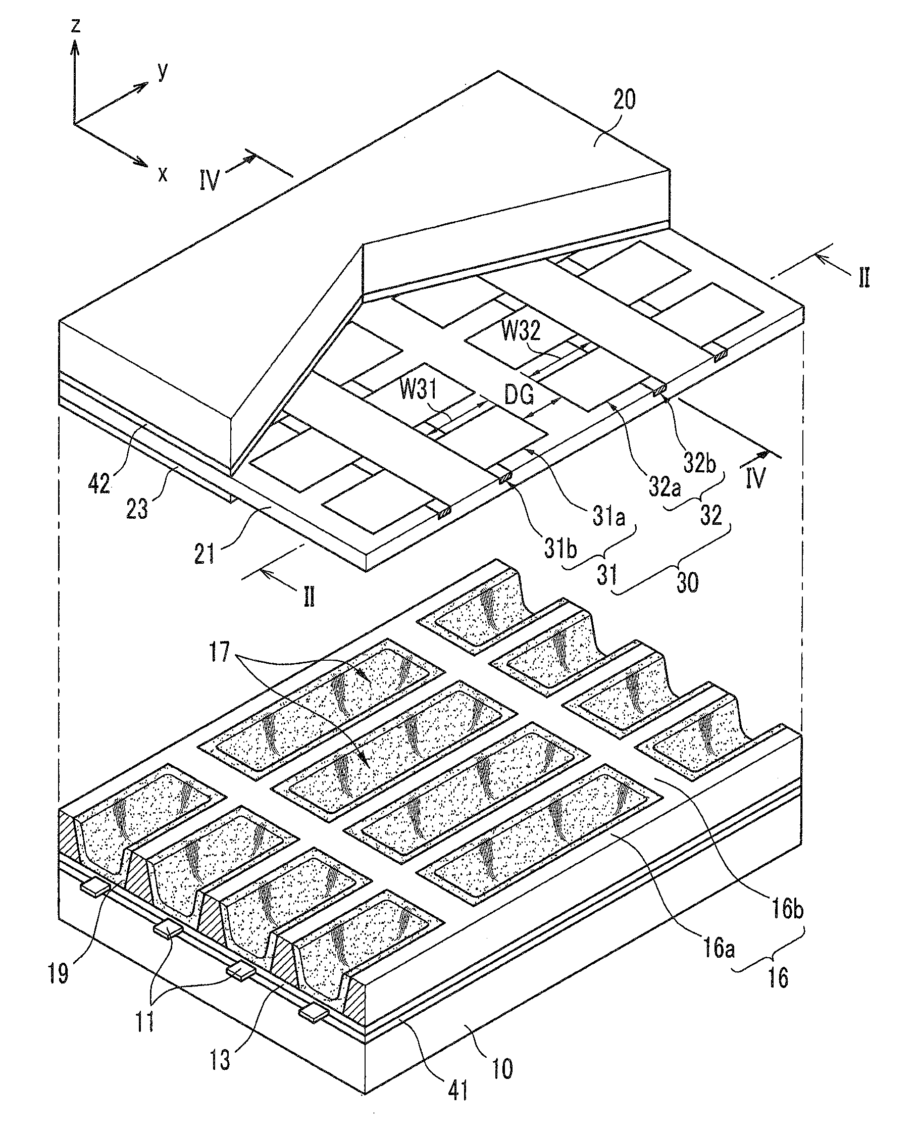
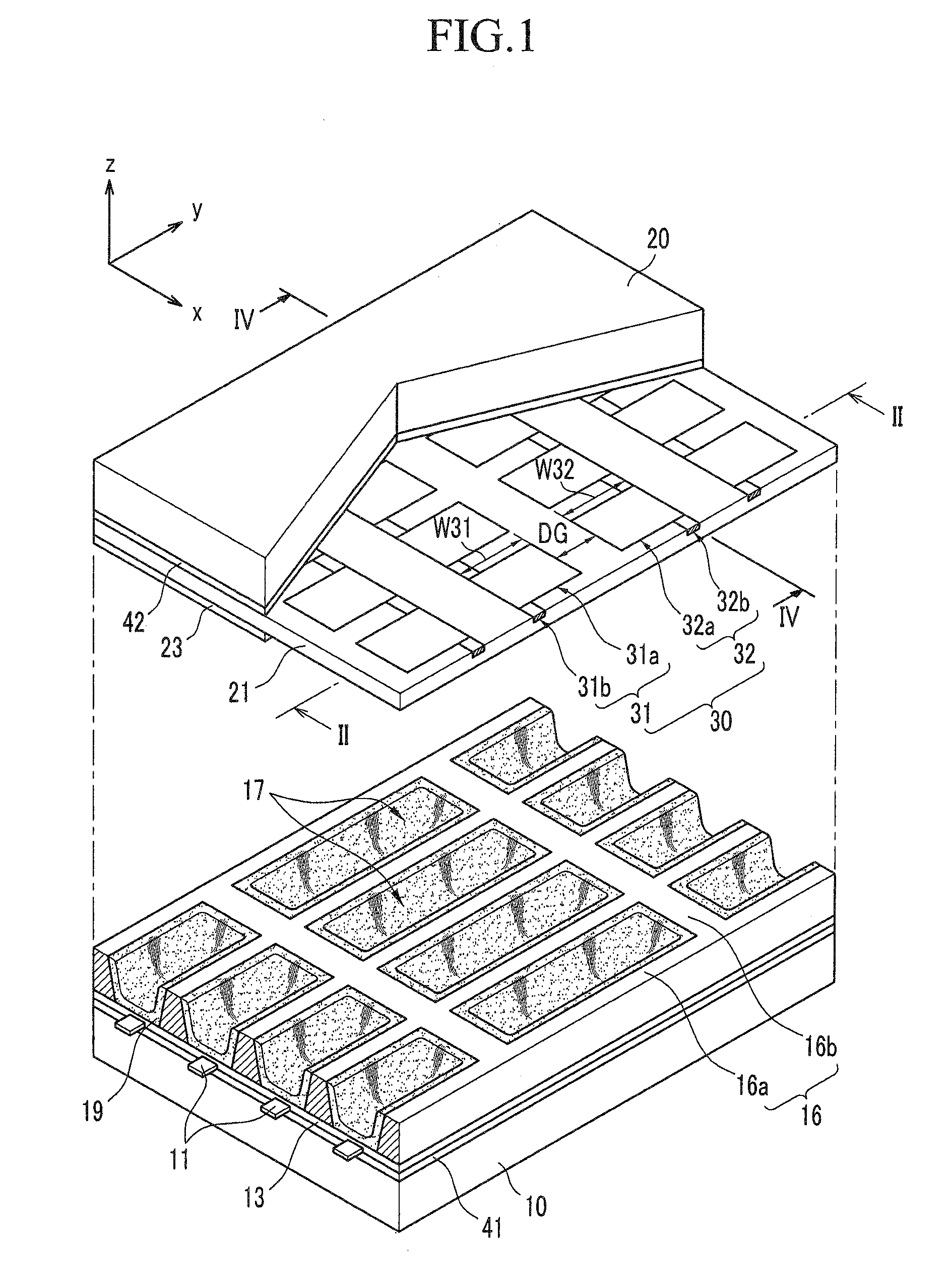
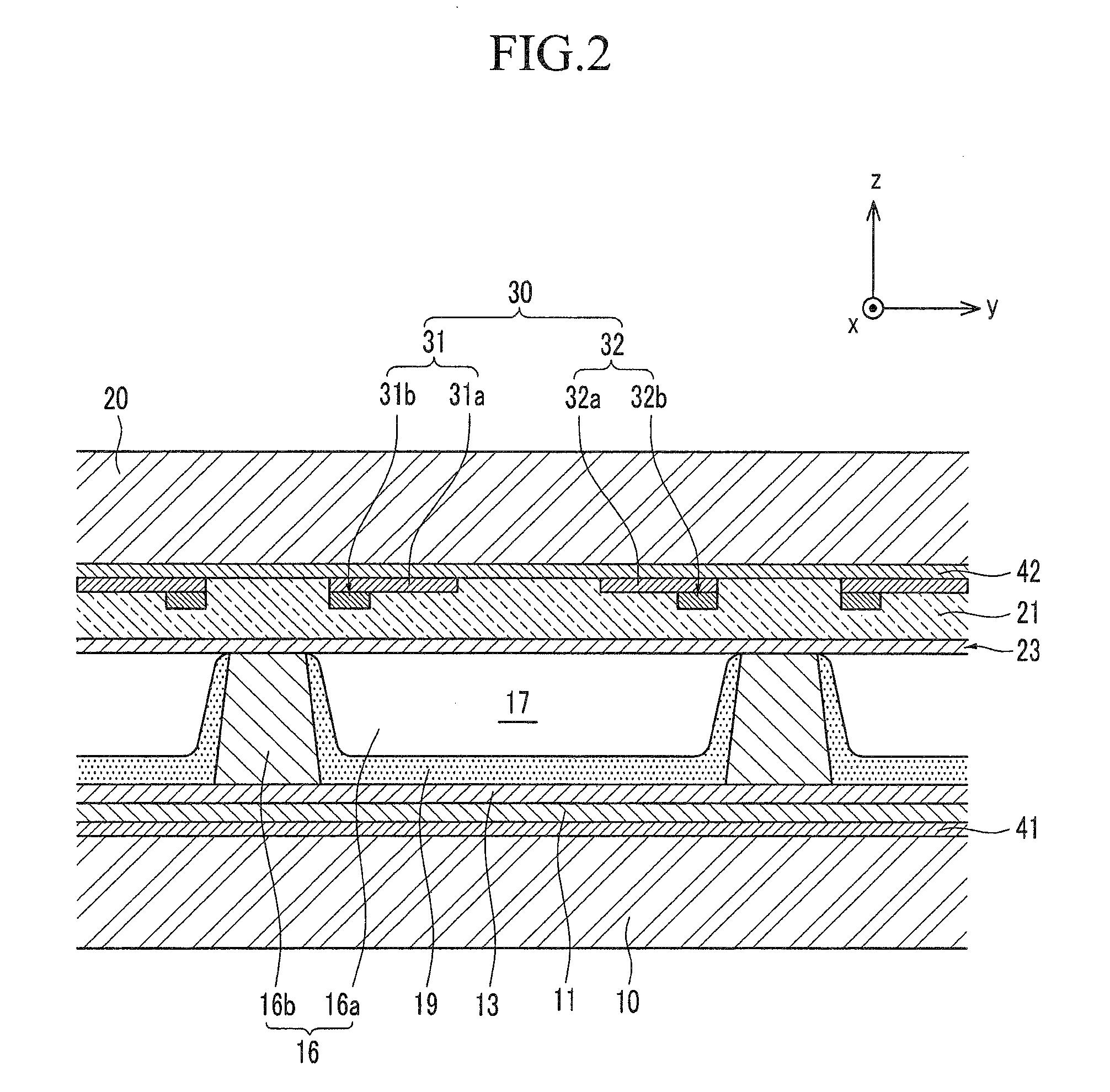
[0044]FIG. 1 is an exploded perspective schematic view of a plasma display panel (PDP) according to an exemplary embodiment of the present invention, and FIG. 2 is a cross-sectional schematic view of the plasma display panel along a line II-II shown in FIG. 1.

[0045]Referring to FIG. 1 and FIG. 2, the PDP according to the exempl...


PUM


Abstract

A plasma display panel (PDP) for preventing (or reducing) a chemical reaction of Na2O of a sodalime glass substrate and a metal of an electrode. The PDP includes first and second substrates, a barrier rib, a phosphor layer, an address electrode, and a display electrode. The first and second substrates are provided to face each other, the barrier rib is provided between the first and second substrates to partition discharge cells, and the phosphor layer is formed in each discharge cell. The address electrode is between the first and second substrate and extending in a first direction. The display electrode is between the first and second substrates and extending in a second direction crossing the first direction. Here, the first substrate and / or the second substrate is a sodalime glass substrate including Na2O, and a frit is between the sodalime glass substrate and the address electrode and / or the display electrode.

Description

CROSS-REFERENCE TO RELATED APPLICATION[0001]This application claims priority to and the benefit of Korean Patent Application No. 10-2007-0120987, filed in the Korean Intellectual Property Office on Nov. 26, 2007, the entire contents of which are incorporated herein by reference.BACKGROUND OF THE INVENTION[0002]1. Field of the Invention[0003]The present invention relates to a plasma display panel (PDP). More particularly, the present invention relates to a PDP for blocking (or reducing) a chemical reaction between a sodalime glass substrate and an electrode.[0004]2. Description of the Related Art[0005]A plasma display panel (PDP) is a display device for realizing an image by gas discharge. That is, the gas discharge generates plasma, the plasma radiates vacuum ultraviolet (VUV) rays, the VUV rays excite phosphors, and the excited phosphors are stabilized to generate red (R), green (G), and blue (B) visible light.[0006]For example, in an alternating current (AC) PDP, address electrode...

Claims


Application Information

Patent Timeline
IPC IPC(8): H01J17/49
CPCH01J11/34H01J11/12H01J5/10H01J5/04
Inventor KWEON, TAE-JOUNG
Owner SAMSUNG SDI CO LTD
Features
  • Generate Ideas
  • Intellectual Property
  • Life Sciences
  • Materials
  • Tech Scout
  • Unparalleled Data Quality
  • Higher Quality Content
  • 60% Fewer Hallucinations
Learn More