[0010]The present invention has been achieved in view of the situation above, and the object is to provide a polycrystalline silicon manufacturing apparatus and manufacturing method that can efficiently produce high-quality polycrystalline silicon.
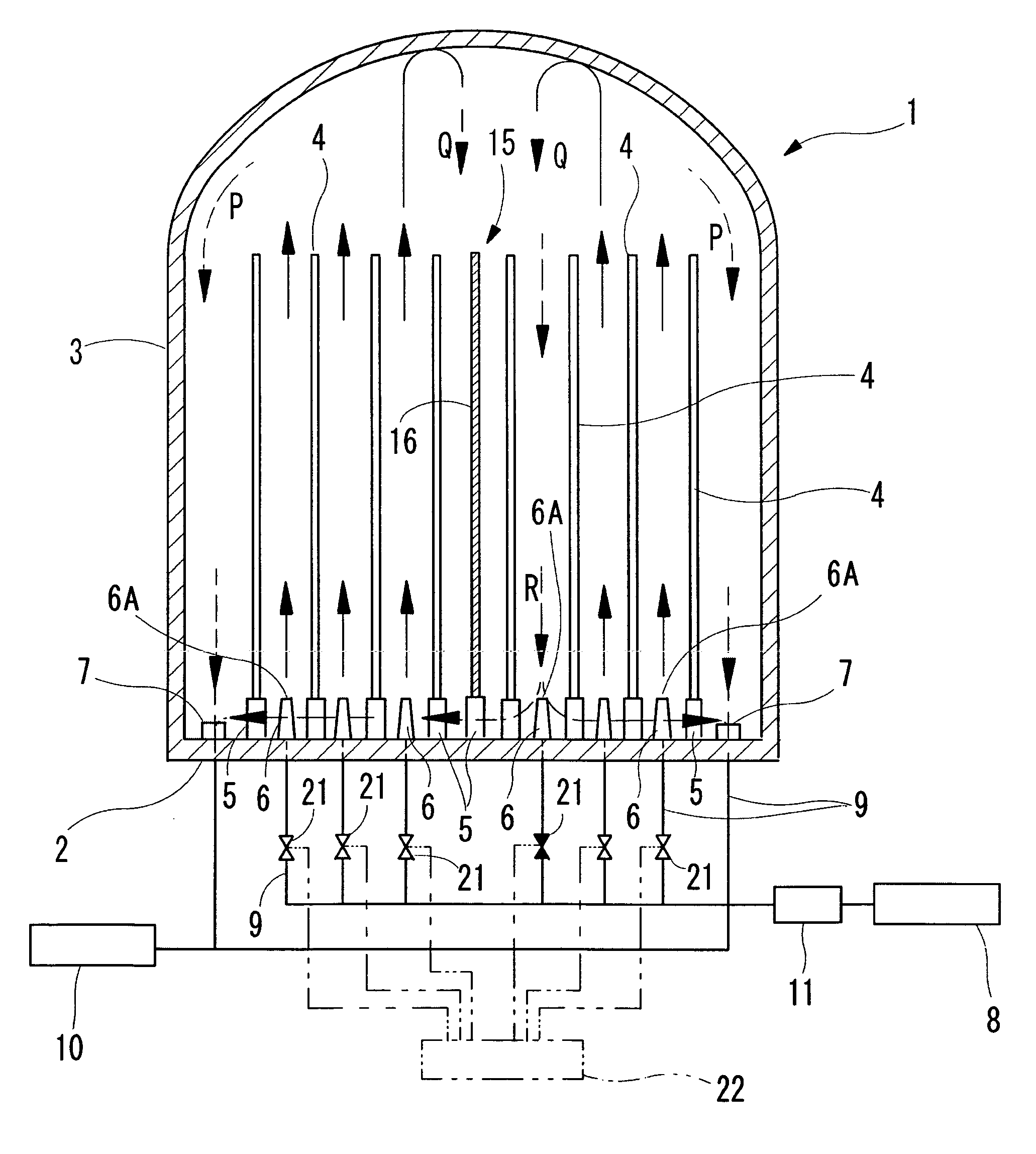
[0012]In the polycrystalline silicon manufacturing apparatus, the raw gas is ejected from the gas supplying ports upward, the upward gas flow comes in contact with the silicon seed rods to deposit the polycrystalline silicon on the surfaces of the silicon seed rods, and the gas after being supplied to deposit the silicon reaches to the ceiling of the reactor and then runs down to the lower side to be exhausted from the gas exhausting ports. At this time, most of the raw gas colliding with the ceiling of the reactor flows toward the outside along the inner circumferential face of the reactor, but in the central portion of the reactor, the flow colliding with the ceiling is reversed without flowing toward the outside to be the downward gas flow, so as to easily cause the downward gas flow to interfere with the upward gas flow rising from the lower side. In particular, since the gas flow adjacent to the center in the reactor is easy to be reversed from the ceiling as it is, there is a tendency that the interference between the gas flows easily occurs. When the interference between the gas flows occurs, the silicon seed rods standing in the reactor swing because the flow direction of the gas becomes unstable. Since the
diameter of silicon rods at an early reaction stage is extremely small as 10 to 20 mm, large swing of the silicon seed rods may result in the breakage of the silicon seed rods.
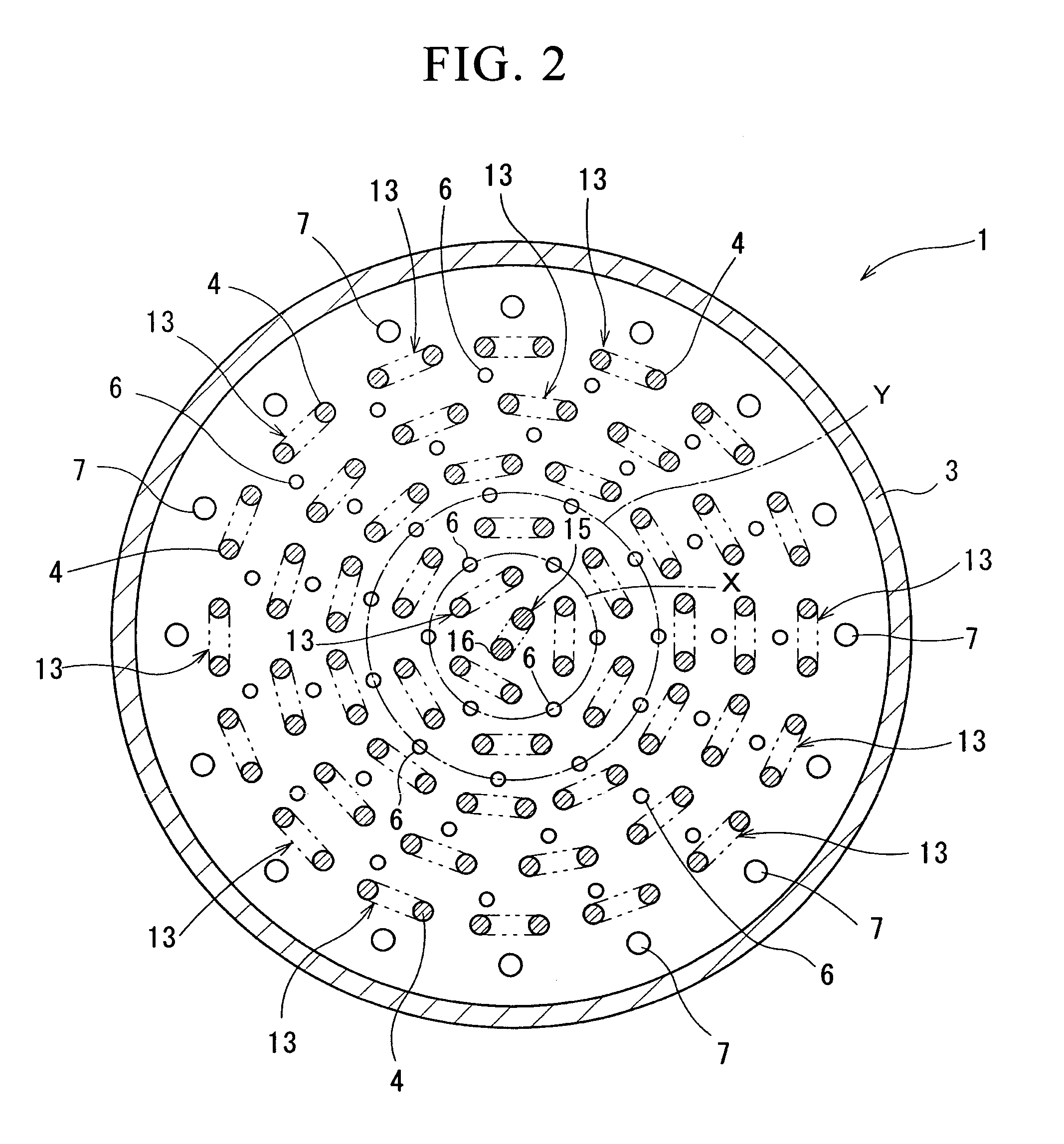
[0013]Therefore, since the valves that are provided on the gas distributing tubes of the gas supplying ports in the adjacent of the center are closed for a predetermined time in order to stop the gas flow from the lower side, the state in which the downward gas flow from the ceiling easily reaches to the inner bottom in the reactor can be guaranteed. Since the posture of the silicon seed rods after the polycrystalline silicon is sufficiently deposited thereon is stable, this control of the valves is performed at an early step of the reaction. Then, the opening or closing of these valves is appropriately controlled in order to prevent the interference between the upward gas flow and the downward gas flow, and the silicon can be grown in the state where gas flow along the periphery of the silicon seed rods is stable. After the growth of the silicon is stabilized, the control may be stopped.
[0015]In this case, the valve controlling device selects the gas supplying ports corresponding to 5 to 15% of the total number of the gas supplying ports from among the gas supplying ports placed on a most inner circumference and a second circumference from the most inner circumference to control the valves of the gas distributing tubes connected to the selected gas supplying ports to be closed for a predetermined time, and after the predetermined time is passed, selects the same pieces of the gas supplying ports from among the gas supplying ports, which are under the opened state, placed on the most inner circumference and the second circumference from the most inner circumference to control the valves of the gas distributing tubes connected to the selected gas supplying ports to be in the
closed state and also controls the valves in the
closed state to be opened. In the method for selecting the gas supplying ports, it is desirable that the gas supplying ports to be closed are selected so that both of two adjacent gas supplying ports on the same circumference are not closed. Then, after the valves of the selected gas supplying ports are closed for a predetermined time, the other gas supplying ports are selected, the opening and closing for the valves of the gas supplying ports are switched, the valves of the selected gas supplying ports are similarly closed for a predetermined time, and these operations are repeated. Since this switching between opening and closing of the valves is performed by an automatic
computer control, the downward gas flow can be led to the space above the gas supplying ports having the closed valves while the raw gas is supplied to the silicon seed rods by a
proper time, and thus the silicon can be appropriately deposited to stabilize the growth of the silicon.
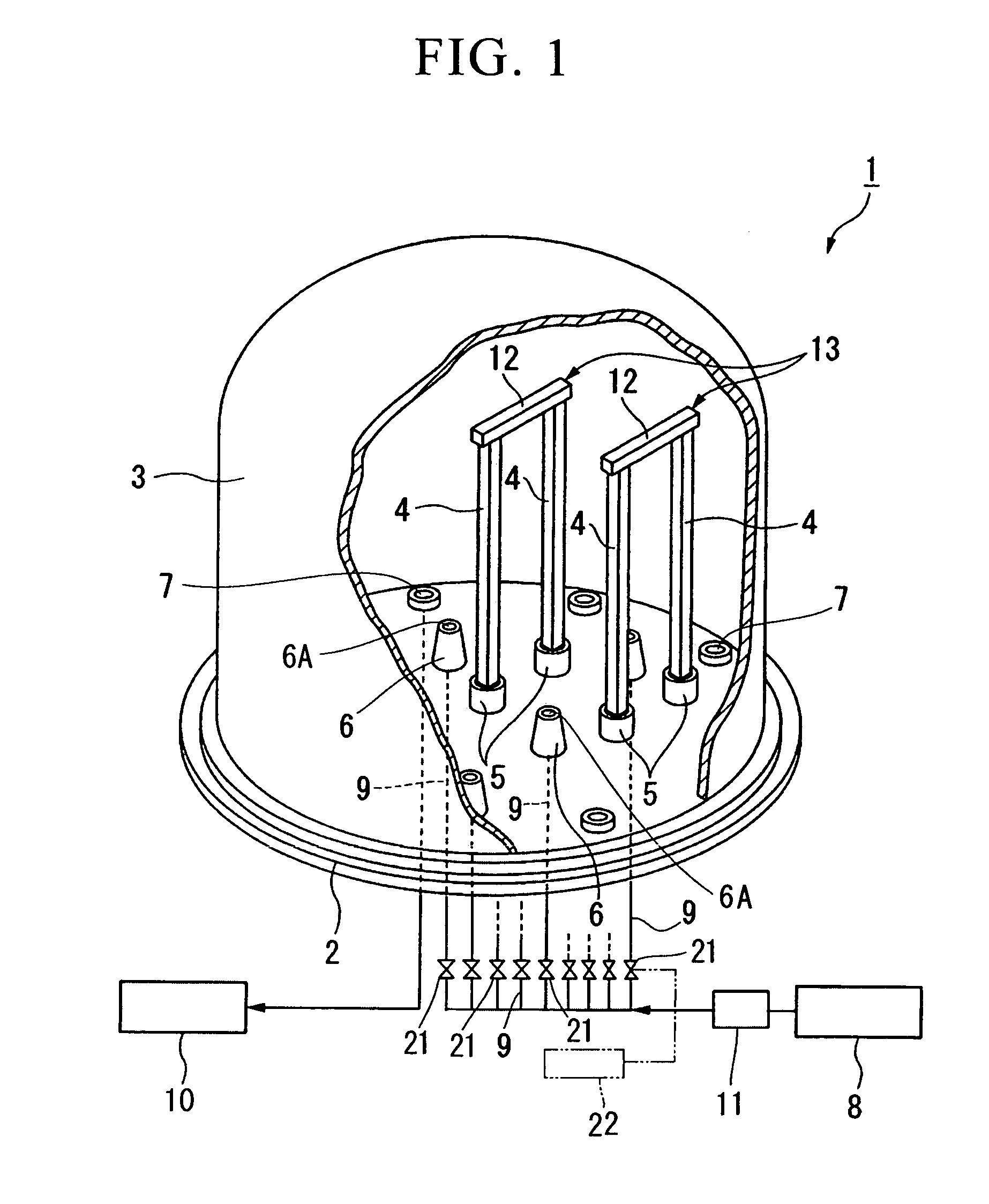
[0017]In the polycrystalline silicon manufacturing apparatus, since the gas supplying ports are arranged at a position upper than the inner bottom of the reactor, a space where the gas is not ejected is formed between the inner bottom of the reactor and the gas supplying ports. Therefore, the falling
exhaust gas flows horizontally through the space and is led to the gas exhausting ports. As a result, the upward flow of the raw gas is not disturbed by the horizontally directional flow as well as the downward flow of the
exhaust gas, and the raw gas can be very stably supplied along the silicon seed rods.
[0020]According to the present invention, since the valves that are provided on the gas distributing tubes of the gas supplying ports in the adjacent of the center of the reactor are closed to stop the gas flow from the lower side at an early stage of the reaction, the state where the downward gas flow easily reaches to the inner bottom in the reactor can be guaranteed. Since the opening or closing of the valves is appropriately controlled to prevent interference between the upward gas flow and the downward gas flow, the silicon can be grown in the state where the gas flow along the periphery of the silicon seed rods is stable and thus high-quality silicon can be manufactured. Moreover, an existing manufacturing apparatus can be applied without changing the scale by only controlling the supply device for raw gas.

