Method for producing a semiconductor device

Inactive Publication Date: 2009-06-11
SHARP KK
View PDF10 Cites 3 Cited by
  • Summary
  • Abstract
  • Description
  • Claims
  • Application Information

AI Technical Summary

Benefits of technology

[0051]According to the method for producing a semiconductor device of this embodiment, because the removal of the halogen is performed such that the halogen i

Problems solved by technology

However, the countermeasure has a problem that the production cost increases because the countermeasure significantly changes the process of forming Au bumps from a conventional process of forming Au bumps and us

Method used


Image

  • Method for producing a semiconductor device
  • Method for producing a semiconductor device
  • Method for producing a semiconductor device

Examples


Embodiment Construction

[0064]A method for producing a semiconductor device according to the present invention will be described in detail below with reference to embodiments shown in the figures.

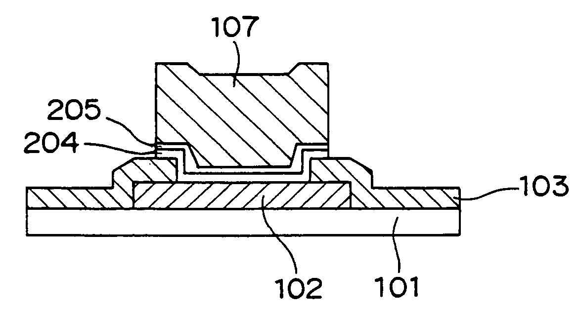
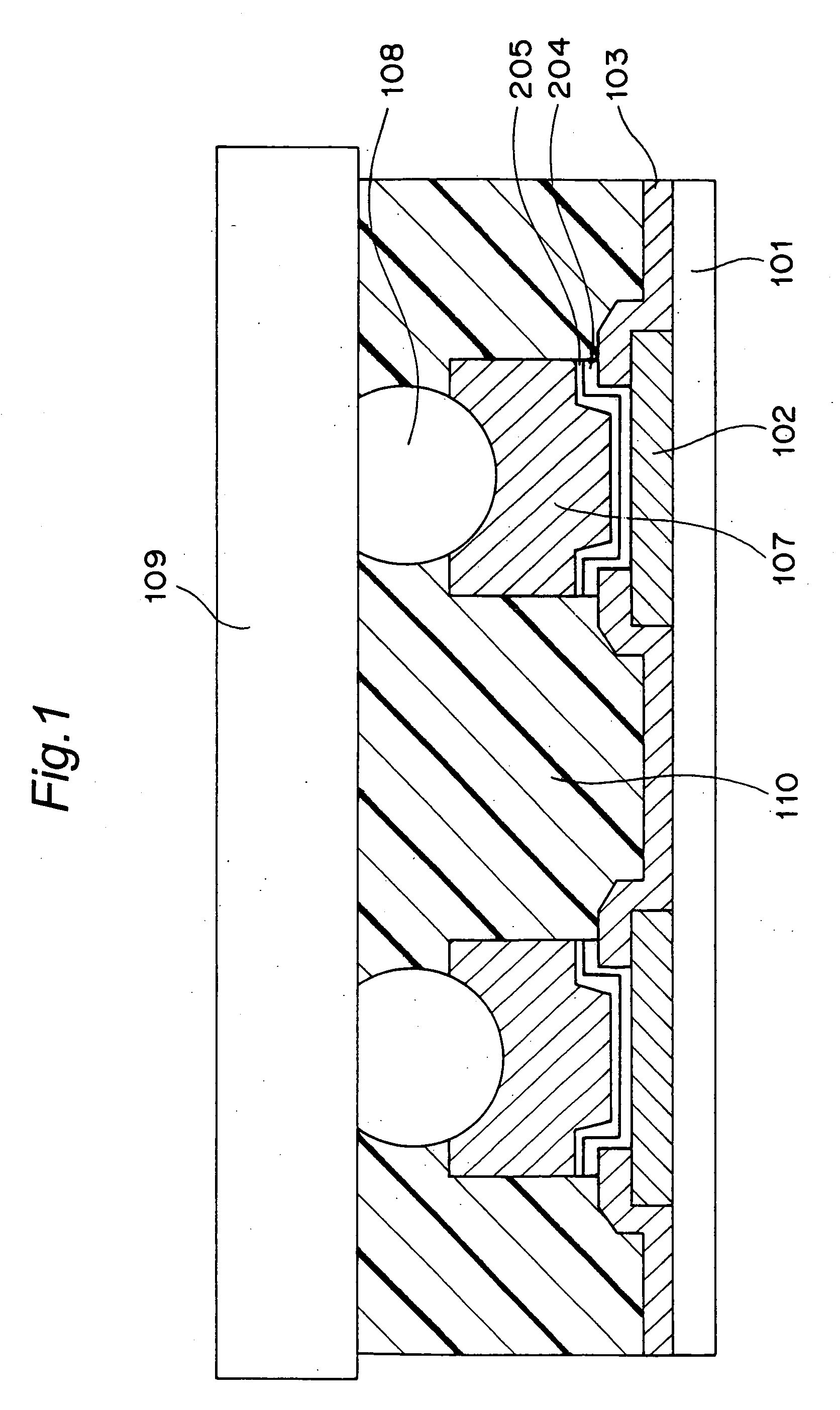
[0065]FIG. 3 is a flow chart of a method for producing a semiconductor device according to an embodiment of the present invention. Each of FIGS. 4A to 4G is a schematic cross-sectional view depicting different steps of the method for producing a semiconductor device. Although only one pad electrode 102 is shown in FIGS. 4A to 4G, several hundreds of pad electrodes 102 are actually formed on the surface of a semiconductor element 101.

[0066]In the method for producing a semiconductor device, first, pad electrodes 102 and a surface protection film 103 are formed on a semiconductor element 101 as shown in FIG. 4A. Openings are formed in the surface protection film 103, and part of the surfaces of the pad electrodes 102 are exposed from the openings.

[0067]Next, at step S101 in FIG. 3, UBM (under bump metal) sputtering ...


PUM


Abstract

At step S101, a TiW film is formed by a sputtering method so as to cover a surface protection film and pad electrodes formed on a surface of a semiconductor element. Subsequently, an Au film is formed on the TiW film. At step S103, Au bumps are formed on the Au film using the Au film as a plating electrode. At step S105, unnecessary parts of the Au film are removed. At step S106, unnecessary parts of the TiW film are removed. At step S107, iodine left in areas where the unnecessary parts of the TiW film have been removed, is removed.

Description

[0001]This nonprovisional application claims priority under 35 U.S.C. §119(a) on Patent Application No(s). 2007-102449 filed in Japan on Apr. 10, 2007, the entire contents of which are hereby incorporated by reference.BACKGROUND OF THE INVENTION[0002]The present invention relates to a method for producing a semiconductor device used for, for example, a semiconductor integrated circuit.[0003]Semiconductor elements tend to reduce in size with becoming finer and increase in the number of pad electrodes by the pursuit of higher functionality. As a result, the pitch of the pad electrodes tends to reduce, and the pitch of the order of 20 μm to 50 μm is a reality.[0004]Furthermore, as a technique of mounting a semiconductor element, there has been established and has been mainstream a technique in which Au bumps are formed on pad electrodes, then the semiconductor element is mounted on a tape via the Au bumps, and then the semiconductor element mounted on the tape is installed in various e...

Claims


Application Information

Patent Timeline
IPC IPC(8): H01L21/60
CPCH01L24/11H01L2224/1147H01L2224/13099H01L2224/16H01L2924/14H01L2924/01078H01L2924/01079H01L2924/01082H01L2924/01033H01L2224/05027H01L2224/05022H01L2924/01006H01L2924/01019H01L2224/05001H01L2224/05572H01L2224/05644H01L24/03H01L24/06H01L24/05H01L2924/00014
Inventor NIE, NORIMITSUHORIO, MASAHIROSAWAI, KEIICHIWATANABE, YUJIKOYAMA, YASUHIROKAWAKAMI, KATSUJI
Owner SHARP KK
Why Eureka
Try Eureka