Packaging apparatus for optical-electronic semiconductors and a packaging method therefor

a technology of optical-electronic semiconductors and packaging apparatus, which is applied in the direction of turning machine accessories, drawing profiling tools, printing, etc., can solve the problems of limited production rate of packaging process, temperature difference between led body and furnace, and inability to easily control heat exchange, etc., to achieve the effect of increasing the production ra

Active Publication Date: 2009-06-18
LITE ON TECH CORP +1
View PDF2 Cites 0 Cited by
  • Summary
  • Abstract
  • Description
  • Claims
  • Application Information

AI Technical Summary

Benefits of technology

[0009]The primary object of the present invention is to provide for a packaging apparatus for optical-electronic semiconductors and a packaging method therefor. The present invention is applied for increasing the production rate.
[0010]Another object of the present invention is to provide a method for improving the heating uniformity of the furnace hot air so as to optimize the stability of the curing quality of the optical-electronic semiconductors.
[0011]A further object of the present invention is to hold the position of the supporting members precisely so as to prevent the supporting members from off-centering.
[0012]In order to achieve the above objects, the present invention provides a packaging apparatus for optical-electronic semiconductors that comprises a mold base, an encapsulating module, and a fixing member. The encapsulating module is used for holding a plurality of columns of molding bodies inside the mold base. There is at least one first air-vent formed on the bottom of the mold base so that the heated air can flow to contact the molding bodies in order to improve the uniformity of heating process. The fixing member is used for positioning a plurality of columns of supporting members connected to the molding bodies so as to solve the off-centering issue of the traditional packaging method. On the other hand, the fixing member provides a supporting and pressing functions as the baking procedure.
[0013]The present invention is provided for increasing the production precision of the optical-electronic semiconductors after the heating process.
[0014]The cost of the process is reduced compare to traditional process because of the optimization of the width of the packaging apparatus.

Problems solved by technology

However, traditional mold only receives one row of LEDs, so the production rate of the packaging process is limited.
Furthermore, the connection metal is inserted in a hole formed by a plastic member that deforms gradually due to friction and usage.
Also, the traditional mold is an enclosed mold and the heated air cannot reach the LED body directly.
Thus, a temperature difference occurs between the LED body and furnace.
Thus, the heat exchange is not easily controlled and the heating accuracy of the LED is low.

Method used


Image

  • Packaging apparatus for optical-electronic semiconductors and a packaging method therefor
  • Packaging apparatus for optical-electronic semiconductors and a packaging method therefor
  • Packaging apparatus for optical-electronic semiconductors and a packaging method therefor

Examples


Embodiment Construction

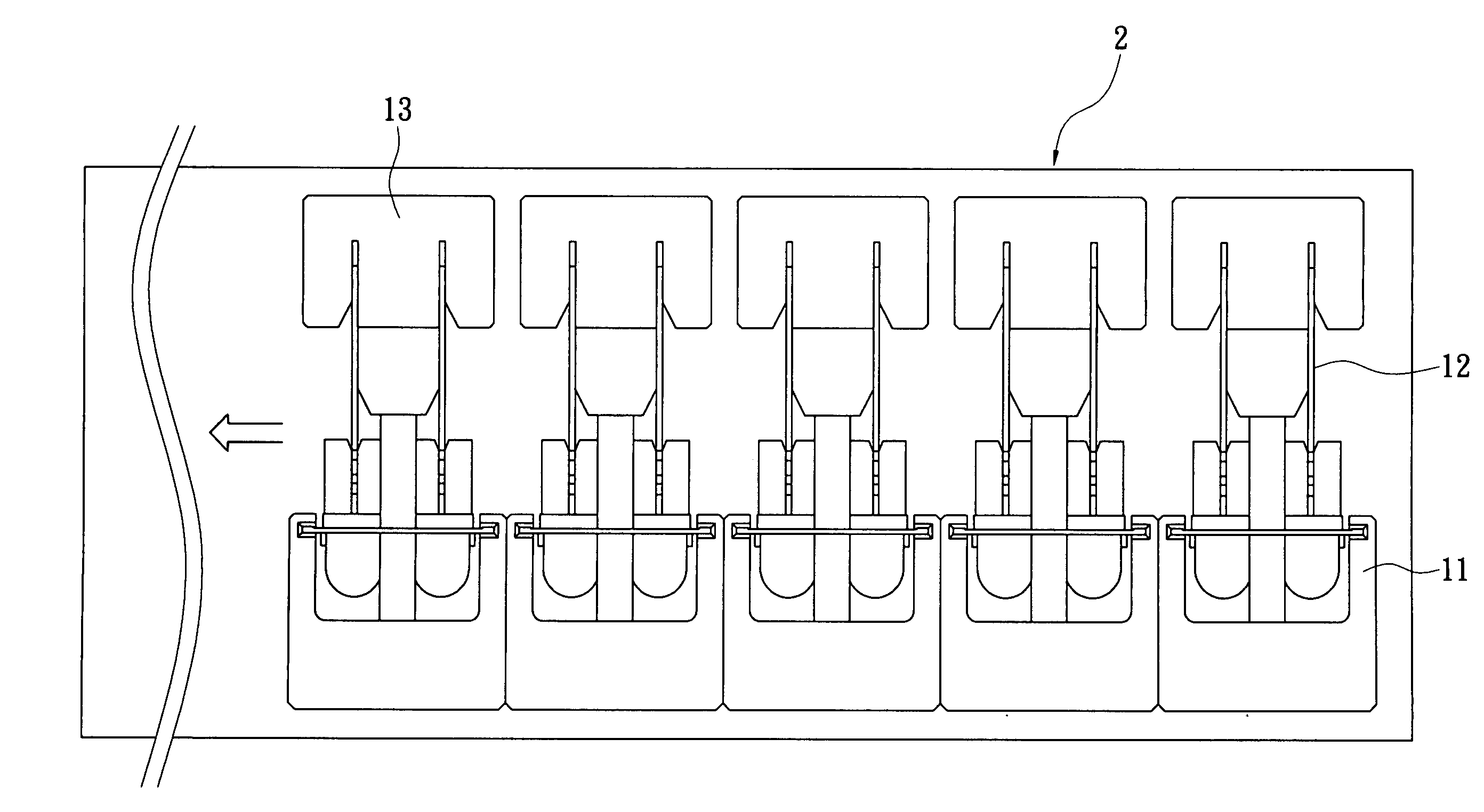
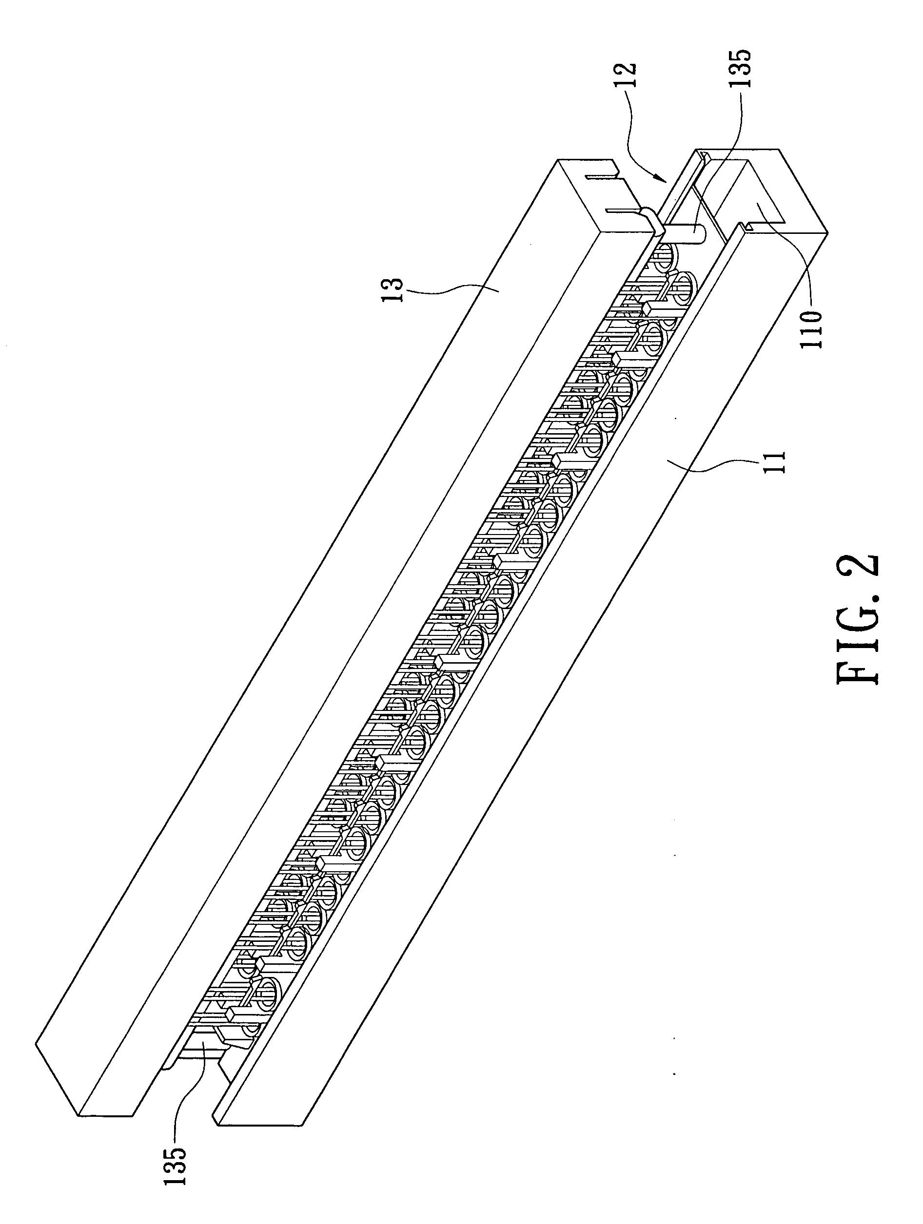
[0023]Please refer to FIGS. 1-7, the invention discloses a packaging apparatus and a packaging method for optical-electronic semiconductors. The apparatus and the method are applied for optical-electronic semiconductors, such as light emitting diodes, receiver chips and etc. The packaging apparatus 1 comprises a mold base 11, an encapsulating module 12 attached to mold base 11, and a fixing member 13 attached to encapsulating module 12. The mold base 11 has a longitudinal receiving space 110 and at least one first air-vent 111 at the bottom thereof. The mold base 11 has a predetermined width W and the first air-vent 111 communicates with the longitudinal receiving space 110. The encapsulating module 12 has a plate 121 attached to mold base 11, a plurality of columns of molding bodies 122 penetratingly mounted on plate 121 and received in the longitudinal receiving space 110, and a plurality of columns of supporting members 123 connected to the molding bodies 122. The fixing member 1...


PUM

PropertyMeasurementUnit
widthaaaaaaaaaa
widthaaaaaaaaaa
sizeaaaaaaaaaa

Abstract

A packaging apparatus for optical-semiconductors includes a mold base having a longitudinal receiving space, an encapsulating module attached to the mold base, and a fixing member attached to the encapsulating module. The bottom of the mold base has at least one air-vent and the mold base has a predetermined width. The encapsulating module includes a plate engaged with the mold base, a plurality of molding bodies penetrating the plate and received in the receiving space, and a plurality of supporting members connected to the molding bodies. The fixing member has a plurality of holding slots to hold the supporting members so that the supporting members are more stable. Furthermore, the width of the mold base is optimized with the dimension of a furnace so that the production rate is increased and the stability of the packaging structure is improved.

Description

BACKGROUND OF THE INVENTION[0001]1. Field of the Invention[0002]The present invention relates to a packaging apparatus and a packaging method for the optical-electronic semiconductors. The invention in particular relates to a packaging apparatus and a packaging method for improving production efficiency and accuracy of optical-electronic semiconductors.[0003]2. Description of Prior Art[0004]Light emitting diodes (LEDs) have characteristics of small-size, and low-energy consumption so that they are commonly used in electronic productions and display applications. For example, LEDs are applied to traffic lights and cellular phones.[0005]For advanced development of the portable device, engineers focus on increasingly smaller-sized packaging method and ever brighter LED intensity. The traditional packaging methods include dispensing process, encapsulating process, the molding process and so on—and Epoxy with good adhesive and forming property is required for each mentioned process. The ...

Claims


Application Information

Patent Timeline
Patent Type & Authority Applications(United States)
IPC IPC(8): H01L23/34H01L21/56H01L33/48H01L33/52H01L33/56H01L33/62
CPCB29C33/303H01L2924/0002H01L2924/00
Inventor SU, CHENG-HONG
Owner LITE ON TECH CORP
Why Eureka
Try Eureka