Compact Power Semiconductor Package and Method with Stacked Inductor and Integrated Circuit Die

a technology of integrated circuit dies and semiconductors, applied in the field of electrical system packaging, can solve the problems of compact integration of power inductor and power controller ic dies

Active Publication Date: 2009-06-25
ALPHA & OMEGA SEMICON INC
View PDF41 Cites 89 Cited by
  • Summary
  • Abstract
  • Description
  • Claims
  • Application Information

AI Technical Summary

Benefits of technology

[0039]As a more specific embodiment, patterning the set of multiple circuit substrates further includes creating, on each circuit substrate, a bottom recess sized to accommodate the power IC die. Creating the bot

Problems solved by technology

As a result, how to compactly integrate the power inductor with the power controller IC die

Method used


Image

  • Compact Power Semiconductor Package and Method with Stacked Inductor and Integrated Circuit Die
  • Compact Power Semiconductor Package and Method with Stacked Inductor and Integrated Circuit Die
  • Compact Power Semiconductor Package and Method with Stacked Inductor and Integrated Circuit Die

Examples


first embodiment

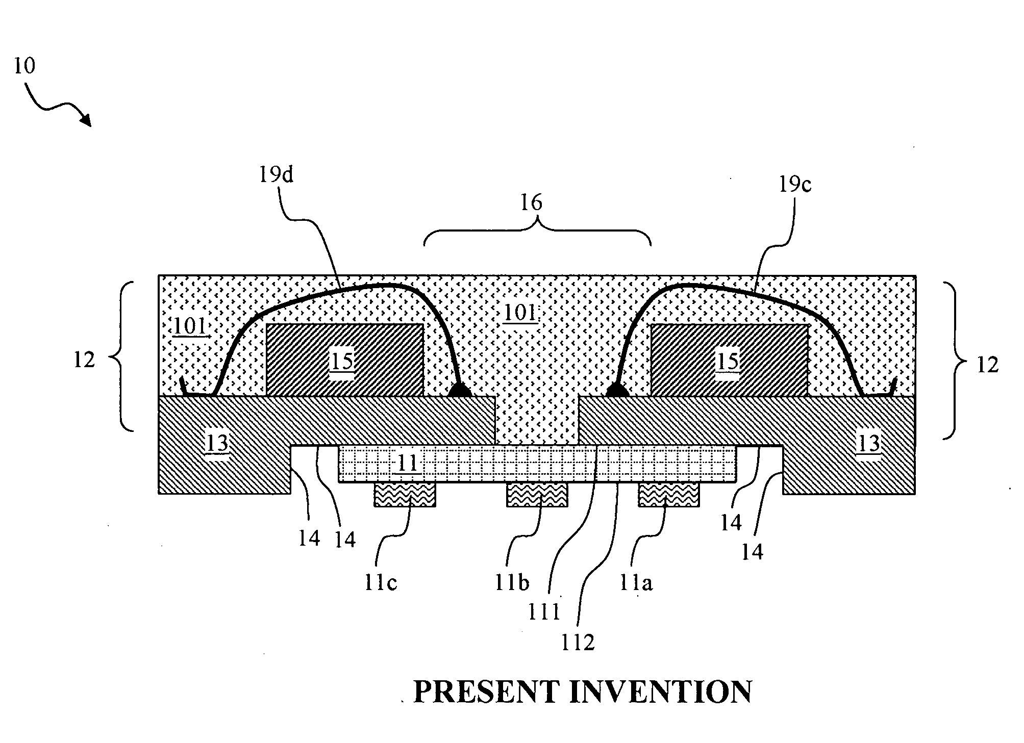
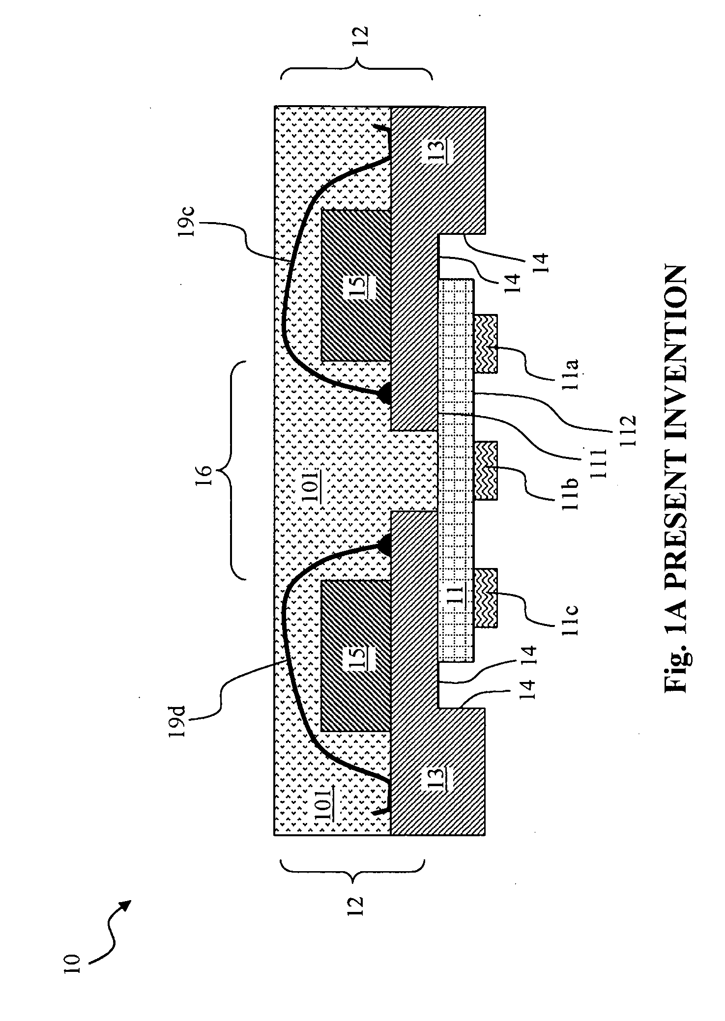
[0060]FIG. 1A through FIG. 1F illustrate the present invention compact power semiconductor package 10 having a bonded stack of power inductor 12, bottom recessed leadframe 13 and power IC die 11 thus exhibiting a reduced package foot print. The bottom recessed leadframe 13 is made, for example by etching, with a bottom recess 14 that should be sized to accommodate the power IC die 11. FIG. 1A is a cross sectional side view of the power semiconductor package 10, FIG. 1B is its top view, FIG. 1C is a top view of an inductor core 15 (e.g., ferrite chip) that is a part of the power inductor 12, FIG. 1D is a top view of bottom half-coil patterned conductive leads 17a through 17g of the bottom recessed leadframe 13, FIG. 1E is a bottom view of the power semiconductor package 10, and FIG. 1F is a bottom view of bottom half-coil patterned conductive leads 17a through 17g mirroring FIG. 1D horizontally.

[0061]The power inductor 12 has a inductor core 15 located atop the bottom recessed leadfr...

third embodiment

[0065]FIG. 3A and FIG. 3B illustrate the bottom views of the present invention using partially sawn leadframes. In the power semiconductor package 30 of FIG. 3A, the bottom recess 14 with partial horizontal sawn edges 31a and 31b can be created by partially sawing the bottom side of a leadframe along a horizontal direction. However, in the power semiconductor package 35 of FIG. 3B, the bottom recess 14 with partial vertical sawn edges 36a and 36b can be created by partially sawing the bottom side of a leadframe along a vertical direction.

fourth embodiment

[0066]FIG. 4A through FIG. 4C illustrate a power semiconductor package 40 using a number of peripheral standoff bumps 43b and 43c at the bottom of leadframe 41 and top half-coil forming interconnection plates 42a through 42h at its top. FIG. 4A is a top view with the encapsulant 101 removed for better visibility of the various internal components. FIG. 4B is the top view of numerous bottom half-coil patterned conductive leads 41a through 41j of leadframe 41. FIG. 4C is a side sectional view of the power semiconductor package 40 along direction A-A.

[0067]Instead of using top half-coil forming bond wires as in FIG. 1A, a number of three dimensionally formed top half-coil forming interconnection plates 42a through 42h, each looping the inductor core 15 from above and further connecting with proper alternative members of the bottom half-coil patterned conductive leads 41a through 41j, are employed to form the inductive coil. Thus, for example, the ends of top half-coil forming interconn...


PUM


Abstract

A power semiconductor package is disclosed with high inductance rating while exhibiting a reduced foot print. It has a bonded stack of power IC die at bottom, a power inductor at top and a circuit substrate, made of leadframe or printed circuit board, in the middle. The power inductor has a inductor core of closed magnetic loop. The circuit substrate has a first number of bottom half-coil forming conductive elements beneath the inductor core. A second number of top half-coil forming conductive elements, made of bond wires, three dimensionally formed interconnection plates or upper leadframe leads, are located atop the inductor core with both ends of each element connected to respective bottom half-coil forming conductive elements to jointly form an inductive coil enclosing the inductor core. A top encapsulant protectively encases the inductor core, the top half-coil forming conductive elements, the bottom half-coil forming conductive elements and the circuit substrate.

Description

CROSS REFERENCE TO RELATED APPLICATIONS[0001]The present invention is a continuation in part application of:[0002]1. application Ser. No. 11 / 986,673 filed on Nov. 23, 2007 and entitled “Semiconductor Power Device Package Having a Lead Frame-Based Integrated Inductor” by Tao Feng et al[0003]2. application Ser. No. 12 / 011,489 filed on Jan. 25, 2008 and entitled “LEAD FRAME-BASED DISCRETE POWER INDUCTOR” by François Hébert et althe entire disclosure of the above is hereby incorporated by reference. The present invention is also related to the following commonly assigned patent applications:[0004]1. application Ser. No. 11 / 729,311, publication# US20080238599 filed on Mar. 27, 2007 and entitled “Chip Scale Power Converter Package Having An Inductor Substrate” Francois Hebert et al[0005]2. application Ser. No. 11 / 818,219, publication# US20080309442 filed on Jun. 12, 2007 and entitled “Semiconductor Power Device Having a Stacked Discrete Inductor structure” Francois Hebert[0006]3. applicat...

Claims


Application Information

Patent Timeline
IPC IPC(8): H01F5/00H01L23/495H01L21/60
CPCH01F17/0033H01L24/49H01L21/4832H01L21/563H01L23/495H01L23/4951H01L23/49548H01L23/49816H01L23/49827H01L23/49861H01L2224/16H01L2224/48091H01L2224/49175H01L2924/01079H01L2924/14H01L2924/15311H01L2924/30107H01F2027/2814H01L24/48H01L2924/00014H01L2224/05573H01L2224/05568H01L2924/19107H01L2224/0616H01L2224/05599H01L2224/45099H01L2224/45015H01L2924/207
Inventor FENG, TAOZHANG, XIAOLIANHEBERT, FRANCOISSUN, MING
Owner ALPHA & OMEGA SEMICON INC
Why Eureka
Try Eureka