Semiconductor memory device maintaining word line driving voltage

a technology of memory device and word line, which is applied in the direction of information storage, static storage, digital storage, etc., can solve the problems of dram operation properties being lowered, data transmission to the cell array is weakened during read and write operations, etc., and achieves the effect of stable driving voltage in the word lin

Inactive Publication Date: 2009-06-25
SK HYNIX INC
View PDF28 Cites 2 Cited by
  • Summary
  • Abstract
  • Description
  • Claims
  • Application Information

AI Technical Summary

Benefits of technology

[0020]The semiconductor memory device according to the present invention can maintain a stable driving voltage in the word line by selectively floating the dummy bit line according to the operation mode.

Problems solved by technology

As such, when the voltage of the word line WL is dropped to less than the VPP level voltage, data transmission to the cell array is weakened during read and write operations.
Therefore, the conventional semiconductor memory device has a problem in that the DRAM operation properties are lowered by the above described defect.

Method used


Image

  • Semiconductor memory device maintaining word line driving voltage
  • Semiconductor memory device maintaining word line driving voltage
  • Semiconductor memory device maintaining word line driving voltage

Examples


Embodiment Construction

[0026]Hereinafter, preferred embodiments of the semiconductor memory device according to the present invention will be described in detail with reference to the accompanying drawings.

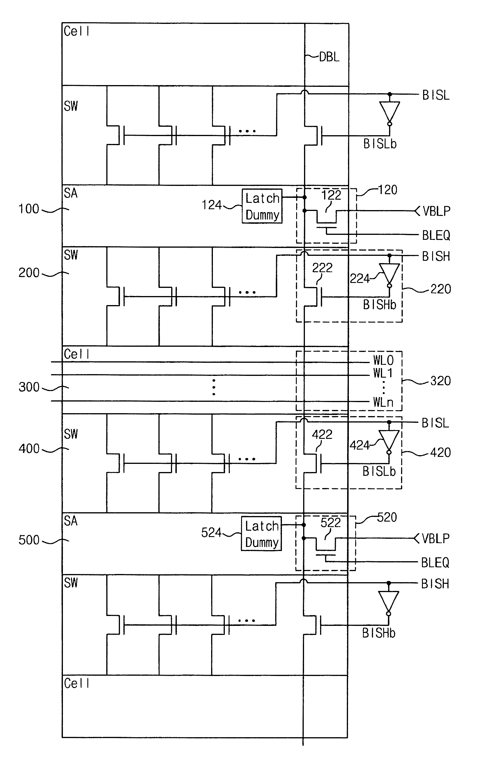
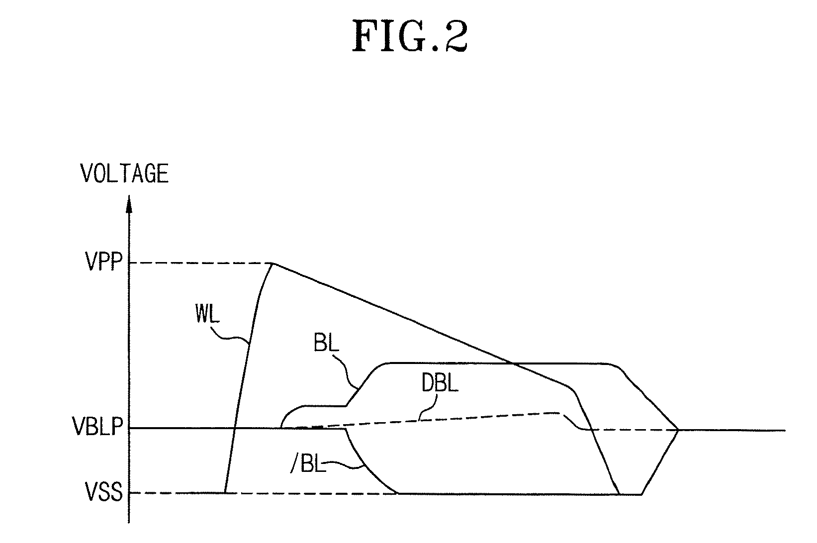
[0027]The present invention discloses a semiconductor memory device which maintains the driving voltage of a word line intersecting a dummy bit line wired in a dummy cell by selectively floating the dummy bit line according to the operation mode. Referring to FIG. 3, the semiconductor memory device according to the present invention includes a cell array 300 in which a plurality of unit cells are arrayed between sense amplifying parts 100 and 500 and switching parts 200 and 400. The switching parts 200 and 400 connect the cell array 300 and the upper and lower sense amplifying parts 100 and 500.

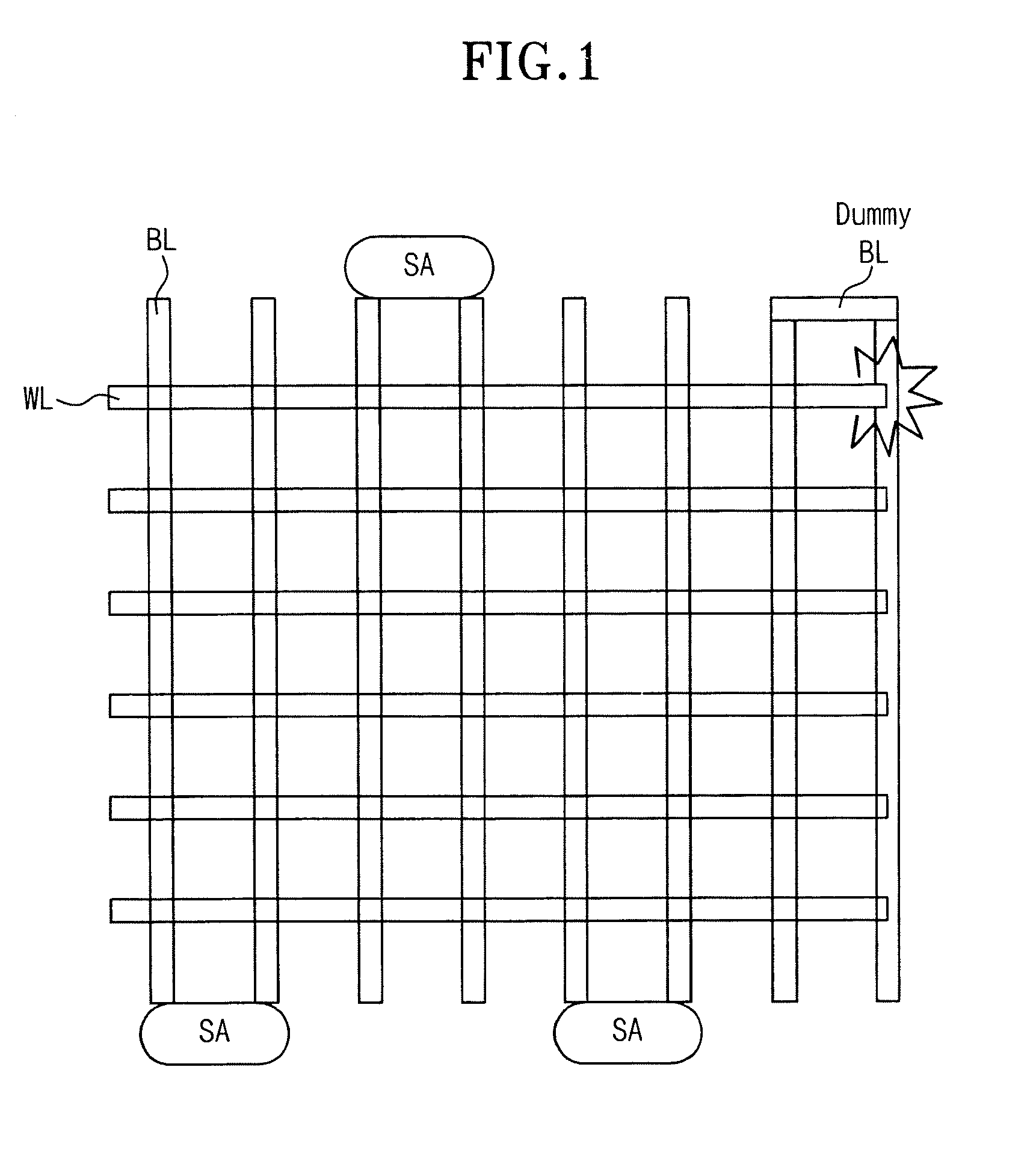
[0028]A cell at the peripheral portion of the cell array 300, in which word lines WL0˜WLn and a dummy bit line DBL intersect, is referred to as a dummy cell 320. Portions at the periphery of the switching parts 2...


PUM


Abstract

A semiconductor memory for maintaining a word line driving voltage includes a cell array and a sense amplifier adjacent to the cell array. A dummy cell is formed at a peripheral portion of the cell array in such a manner that a dummy bit line and a word line intersect. A control circuit switches the connection state between a first section of the dummy bit line passing through the cell array and a second section of the dummy bit line passing through the sense amplifier. The connection state switches according to the operation mode of the cell array. The dummy bit line is floated when the operation mode is an active mode and a precharge voltage is provided to the dummy bit line when the operation mode is a precharge mode.

Description

CROSS-REFERENCE TO RELATED APPLICATIONS[0001]The present application claims priority to Korean patent application number 10-2007-0134652 filed on Dec. 20, 2007, which is incorporated herein by reference in its entirety.BACKGROUND OF THE INVENTION[0002]The present invention relates to a semiconductor memory device, and more particularly to a semiconductor memory device for selectively floating a dummy bit line based on the operation mode of the cell array.[0003]As shown in FIG. 1, a typical DRAM semiconductor memory device includes bit lines BL and word lines WL. The bit lines and the word lines WL intersect to form the pattern shown in FIG. 1. In a DRAM semiconductor memory device cell arrays include a plurality of unit cells. Each unit cell consists of a transistor and a capacitor. A bit line sense amplifier SA senses and amplifies respective signals of a bit line pair BL and / BL.[0004]The following describes the operation of the semiconductor memory device when in active mode: the...

Claims


Application Information

Patent Timeline
Patent Type & Authority Applications(United States)
IPC IPC(8): G11C7/00
CPCG11C11/4085G11C11/4099G11C11/4094H10B12/00
Inventor WON, HYUNG SIK
Owner SK HYNIX INC
Why Eureka
Try Eureka