

Printed wiring board and printed circuit board unit
- Summary
- Abstract
- Description
- Claims
- Application Information
AI Technical Summary
Benefits of technology
Problems solved by technology
Method used
Image

Examples
first embodiment
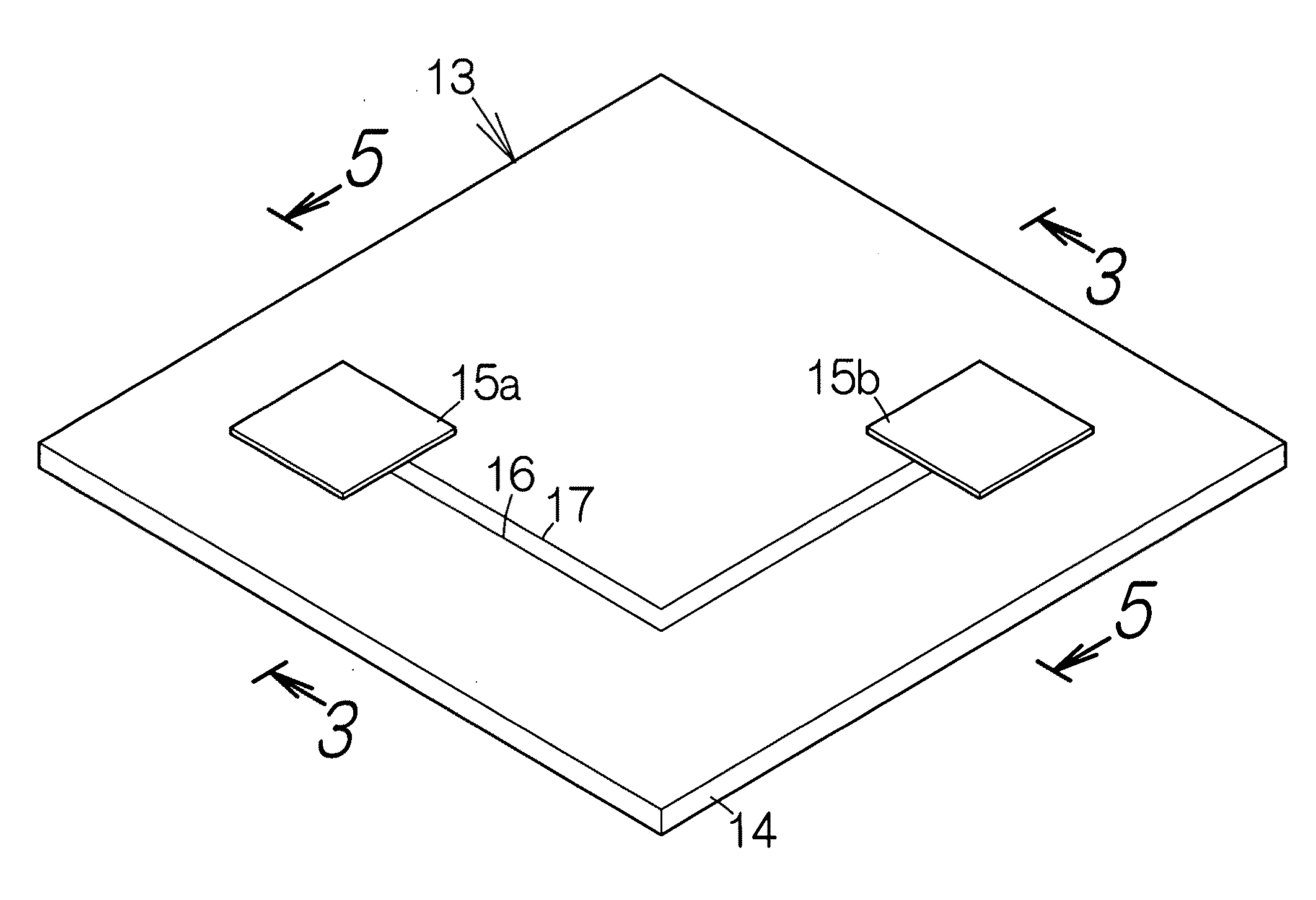
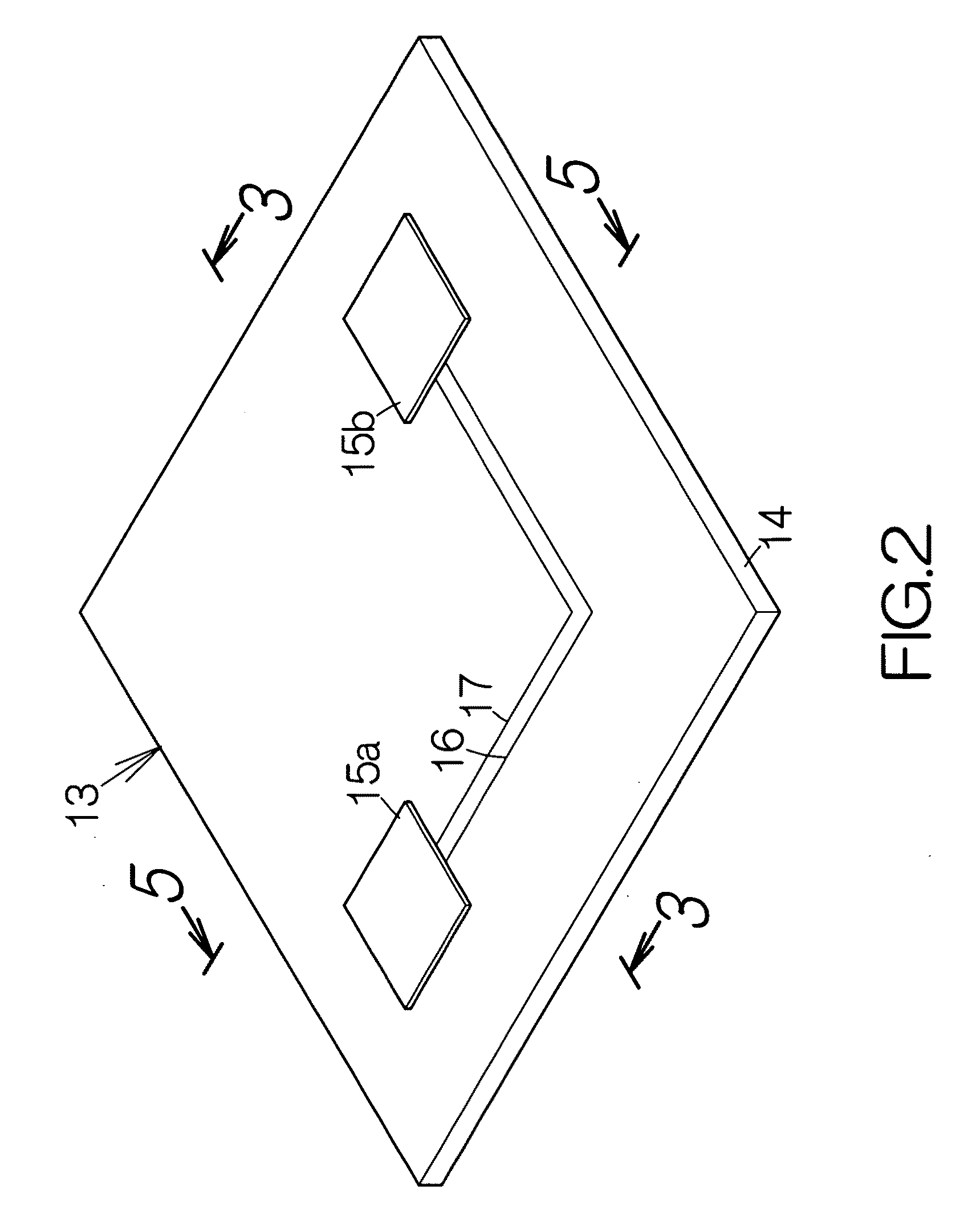
[0026]FIG. 3 schematically illustrates the printed wiring board 14 according to the present invention. The printed wiring board 14 includes a core resin layer 21. Insulating layers 22 are formed on the front and back surfaces of the core resin layer 21, respectively. The core resin layer 21 and the insulating layers 22 each include a body 23 made of resin such as an epoxy resin, for example. The core resin layer 21 has rigidity sufficient to maintain its shape by itself. The core resin layer 21 and the insulating layers 22 each have a thickness of 100 μm to 20 μm approximately, for example.
[0027]A glass fiber cloth 24 is embedded within the body 23. The glass fiber cloth 24 has a thickness of 30 μm approximately, for example. Referring also to FIG. 4, the glass fiber cloth 24 is woven from warp yarns 26 extending in parallel one another and weft yarns 27 extending in parallel one another. Here, the warp yarns 26 intersect with the weft yarns 27 at right angles. The warp yarns 26 are...
second embodiment
[0038]FIG. 6 schematically illustrates a printed wiring board 14a according to the present invention. In the printed wiring board 14a, an interval P3 is defined between the centerlines of the two outermost ones of adjacent three of the warp yarns 26 extending in parallel one another. The width W1 and the width W2 are set equal to or larger than the interval P3. Specifically, the interval P3 is set equal to or larger than twice the interval P1. Likewise, an interval P4 is defined between the centerlines of the two outermost ones of adjacent three of the weft yarns 27 extending in parallel one another. The width W1 and the width W2 are set equal to or larger than the interval P4. Specifically, the interval P4 is set equal to or larger than twice the interval P2. The interval P3 and the interval P4 are set at 200 μm approximately, for example. Here, the width W1 and the width W2 are set at 250 μm approximately, for example. Like reference numerals are attached to the structure or compo...
third embodiment
[0041]FIG. 7 schematically illustrates a printed wiring board 14b according to the present invention. In the printed wiring board 14b, the width W1 and the width W2 are set equal to or larger than the aforementioned P1 (P2) in the same manner as described above. Simultaneously, the width W1 and the width W2 are set equal to the integer times the interval P1 (P2). Here, the width W1 and the width W2 are set equal to twice the interval P1 (P2). Specifically, the width W1 and the width W2 are set at 200 μm approximately. Like reference numerals are attached to the structure or components equivalent to those of the printed wiring boards 14, 14a.
[0042]In the printed wiring board 14b, when the width W1 and the width W2 are set equal to integer times the interval P1 (P2), twice the interval P1 (P2), in this case, each of the first and second wiring patterns 16, 17 is reliably located over a region containing at least a pair of the first regions 28 (31) and a pair of the second regions 29 ...
PUM
| Property | Measurement | Unit |
|---|---|---|
| Electrical conductor | aaaaa | aaaaa |
| Width | aaaaa | aaaaa |
Abstract
Description
Claims
Application Information