Contiguous microlens array, method of fabricating the same and photomask for defining the same

a technology of contiguous microlens array and photomask, which is applied in the field of image recording apparatus, can solve the problems of reducing the recording accuracy of images, unable to achieve light focusing, and integrating the conventional microlens array with other elements

Active Publication Date: 2009-07-09
MARLIN SEMICON LTD
View PDF6 Cites 29 Cited by
  • Summary
  • Abstract
  • Description
  • Claims
  • Application Information

AI Technical Summary

Benefits of technology

[0008]Accordingly, this invention provides a contiguous microlens array that can solve the issue of poor focusing in the prior art and may even allows the peripheral part of an image to be recorded accurately without position shifts of some interconnect structures.

Problems solved by technology

Moreover, because neighboring microlenses 110 are not connected with each other and there are planar sections without a focusing effect between them, the incident light are not fully collected so that the light focusing is not quite effective.
There is also an issue on the integration of the conventional microlens array with other elements in a image recording apparatus, which is described below with a CMOS image recording apparatus having photodiodes as photosensing devices as an example.
However, this makes the exit light 50a from the microlens 110 partially blocked by the second-level interconnect layer 24 and thus lowers the recording accuracy of the image.

Method used


Image

  • Contiguous microlens array, method of fabricating the same and photomask for defining the same
  • Contiguous microlens array, method of fabricating the same and photomask for defining the same
  • Contiguous microlens array, method of fabricating the same and photomask for defining the same

Examples


first embodiment

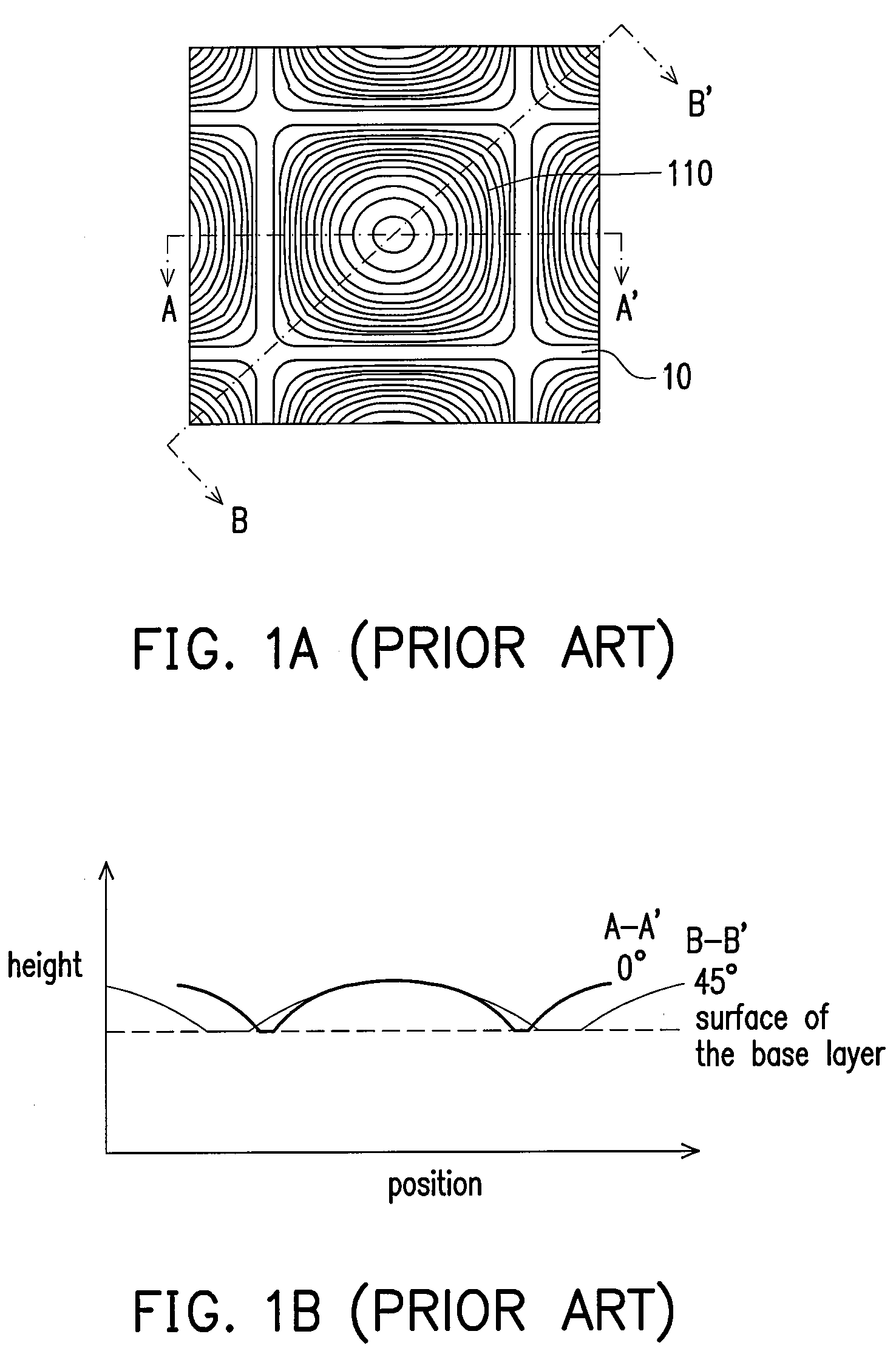
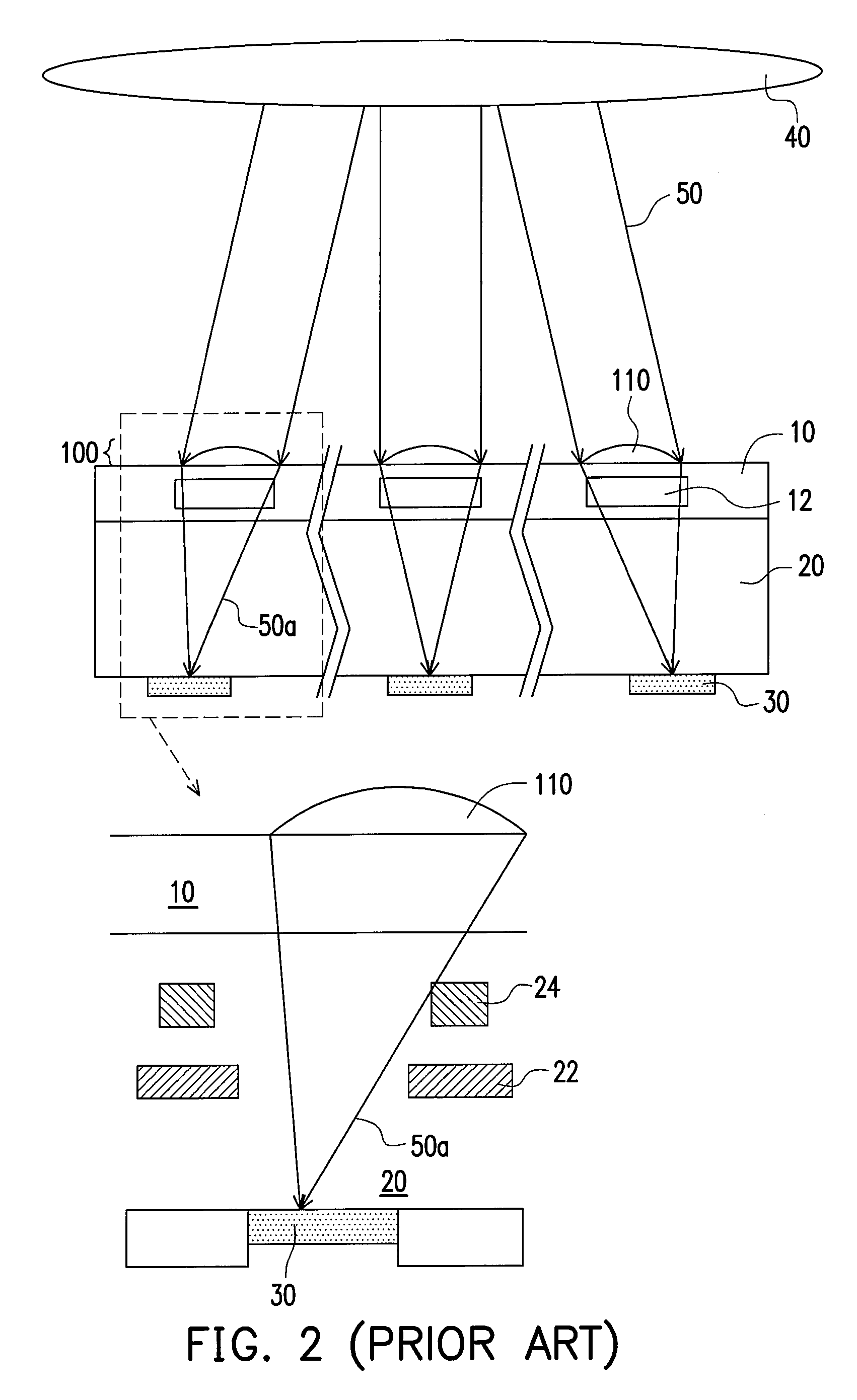
[0040]In the 1st embodiment of the invention, each microlens is substantially symmetric in any vertical cross-sectional view. A microlens in the central part of the microlens array is aligned with the corresponding photosensing device, and a microlens in the at least one peripheral part of the same is laterally shifted relative to the corresponding photosensing device so that light is focused on the latter. Since FIG. 2 has illustrated such a design, the latter figures relating to the first embodiment do not show again the arrangements of the microlenses in different parts of the microlens array relative to the photosensing devices.

[0041]Moreover, since a microlens in the central part of the array is aligned with the corresponding photosensing device, the photoresist pattern as a precursor of a microlens in the central part and the photomask pattern for defining a microlens in the central part both are aligned with the corresponding photosensing device. Since a microlens in the peri...

second embodiment

[0061]In the second embodiment of this invention, each microlens is aligned with the corresponding photosensing device, a microlens in a central part of the microlens array is substantially symmetric in any vertical cross-sectional view, and a microlens in the peripheral part of the microlens array has an asymmetric vertical cross section.

[0062]A CMOS image recording apparatus including photodiodes as the photosensing devices is taken as an example again in the second embodiment. FIG. 6 schematically shows a part of an example of such a CMOS image recording apparatus. The structure of the CMOS image recording apparatus is similar to that shown in FIG. 2 except the shapes and positions of microlenses 610a / b / c in the microlens array 600. Specifically, the microlens array 600 is formed on a transparent base layer 10, which includes a color filter array 12 and other functional layers and is disposed on a multi-level interconnect structure 20 including a first-level interconnect layer 22...


PUM

PropertyMeasurementUnit
incident angleaaaaaaaaaa
exit angleaaaaaaaaaa
temperatureaaaaaaaaaa

Abstract

A contiguous microlens array including a plurality of contiguous microlenses is described. Each microlens has substantially circular contours at the heights higher than the connection sections of the microlens with neighboring microlenses, and has substantially partially circular contours at the heights on the connection sections adjacent to the neighboring microlenses. The shape of the curved surface of a microlens in the microlens array is selectively adjusted according to its position in the array and the incident angle of light incident thereto.

Description

BACKGROUND OF THE INVENTION[0001]1. Field of Invention[0002]This invention relates to an image recording apparatus, and more particularly to a contiguous microlens array, a method of fabricating the same and a photomask for defining the same, which can be applied to any image recording apparatus that requires focusing light on photosensing devices.[0003]2. Description of Related Art[0004]In a semiconductor-type image recording apparatus like a charge-coupled device (CCD) or CMOS image recording apparatus, a microlens array is often disposed over the array of photosensing devices to enhance the sensitivity of the same, wherein one microlens focuses light on one photosensing device.[0005]FIG. 1A is a local contour plot of a conventional microlens array, and FIG. 1B shows the height variations of one microlens in two vertical cross-sectional views at different angles. Because a microlens 110 is formed by reflowing a square photoresist pattern formed on a based layer 10, the shapes of t...

Claims


Application Information

Patent Timeline
Patent Type & Authority Applications(United States)
IPC IPC(8): G02B3/08B29D11/00G03F1/00
CPCB29D11/00365G02B3/0018G03F7/40G02B5/201G02B3/0056
Inventor LIN, YU-TSUNGWU, HSIN-PINGKAO, HUNG-CHAOWANG, MING-I
Owner MARLIN SEMICON LTD
Why Eureka
Try Eureka