

High-frequency circuit having filtering function and reception device
- Summary
- Abstract
- Description
- Claims
- Application Information
AI Technical Summary
Benefits of technology
Problems solved by technology
Method used
Image

Examples
first embodiment
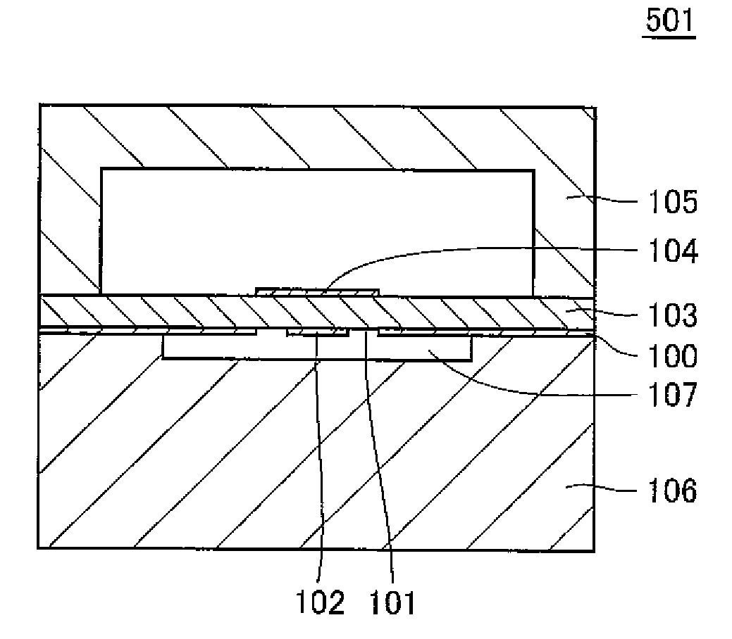
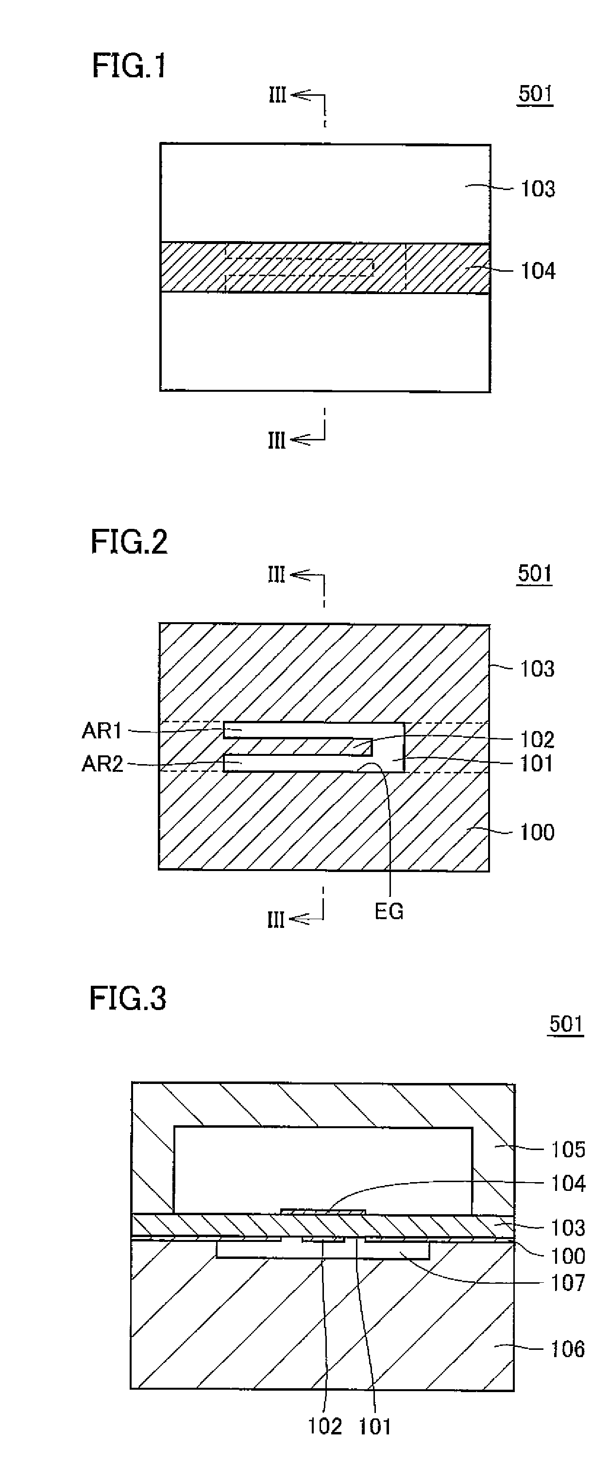
[0043]FIG. 1 is a diagram showing a configuration on a surface of a dielectric substrate in a high-frequency circuit according to a first embodiment of the present invention. FIG. 2 is a diagram showing a configuration on a back surface of the dielectric substrate in the high-frequency circuit according to the first embodiment of the present invention. In FIGS. 1 and 2, dotted lines show patterns in the surface and in the back surface of the dielectric substrate, respectively.
[0044]FIG. 3 is a cross-sectional view of the high-frequency circuit according to the first embodiment of the present invention along the line III-III in FIGS. 1 and 2.
[0045]Referring to FIGS. 1 to 3, a high-frequency circuit 501 includes a ground conductor 100, a pattern cut-out portion 101, a stub 102, a dielectric substrate 103, a microstrip line 104, a frame 105, and a chassis 106.
[0046]For example, dielectric substrate 103 has a thickness of 500 μm and a dielectric constant of 3.33. Microstrip line 104 is ...
second embodiment
[0062]The present embodiment relates to a high-frequency circuit in which one stub is additionally provided as compared with the high-frequency circuit according to the first embodiment. The high-frequency circuit here is the same as the high-frequency circuit according to the first embodiment except for the features described below.
[0063]FIG. 5 is a diagram showing a configuration on a surface of a dielectric substrate in a high-frequency circuit according to the second embodiment of the present invention. FIG. 6 is a diagram showing a configuration on a back surface of the dielectric substrate in the high-frequency circuit according to the second embodiment of the present invention. In FIGS. 5 and 6, dotted lines show patterns in the surface and the back surface of the dielectric substrate, respectively.
[0064]FIG. 7 is a cross-sectional view of the high-frequency circuit according to the second embodiment of the present invention along the line VII-VII in FIGS. 5 and 6.
[0065]Refer...
third embodiment
[0076]The present embodiment relates to a high-frequency circuit in which a coupled-line is formed in a microstrip line as compared with the high-frequency circuit according to the second embodiment. The high-frequency circuit here is the same as the high-frequency circuit according to the second embodiment except for the features described below.
[0077]FIG. 11 is a diagram showing a configuration on a surface of a dielectric substrate in a high-frequency circuit according to the third embodiment of the present invention. FIG. 12 is a diagram showing a configuration on a back surface of the dielectric substrate in the high-frequency circuit according to the third embodiment of the present invention. In FIGS. 11 and 12, dotted lines show patterns on the surface and the back surface of the dielectric substrate, respectively.
[0078]FIG. 13 is a cross-sectional view of the high-frequency circuit according to the third embodiment of the present invention along the line XIII-XIII in FIGS. 1...
PUM
 Abstract
Description
Claims
Application Information