Line Head and Image Forming Device Using the Same

a line head and image forming technology, applied in printing and other directions, can solve the problems of troublesome wiring connections, image quality degradation, and further complicated wiring connections between light emitting elements and drive circuits, and achieve the effect of simplifying wiring connections

Inactive Publication Date: 2009-07-23
SEIKO EPSON CORP
View PDF6 Cites 1 Cited by
  • Summary
  • Abstract
  • Description
  • Claims
  • Application Information

AI Technical Summary

Benefits of technology

[0010]In view of these problems, the present invention provides a line head and an image forming device using the line head that simplify wiring con

Problems solved by technology

Therefore, if the technology of JP-A-2004-209777 is used as it is, there is a problem in that a latent image different from the original image in the rotational direction of the photoconductor drum is formed, and the image quality is therefore degraded.
Further, in a line head having a number of light emitting elements arranged in the X and Y directions of the substrate as shown in FIG. 8, since the wiring connections be

Method used


Image

  • Line Head and Image Forming Device Using the Same
  • Line Head and Image Forming Device Using the Same
  • Line Head and Image Forming Device Using the Same

Examples


Embodiment Construction

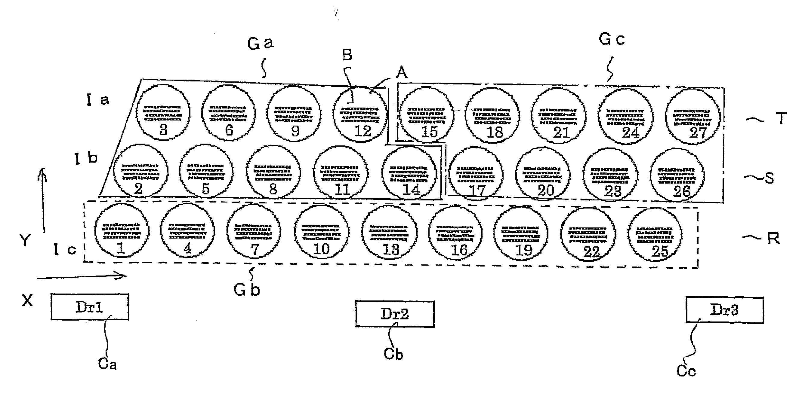
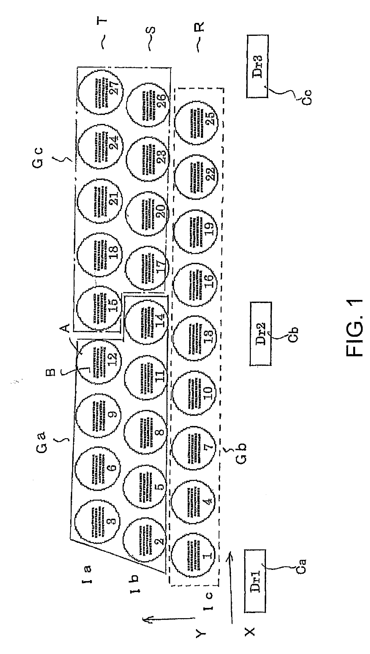
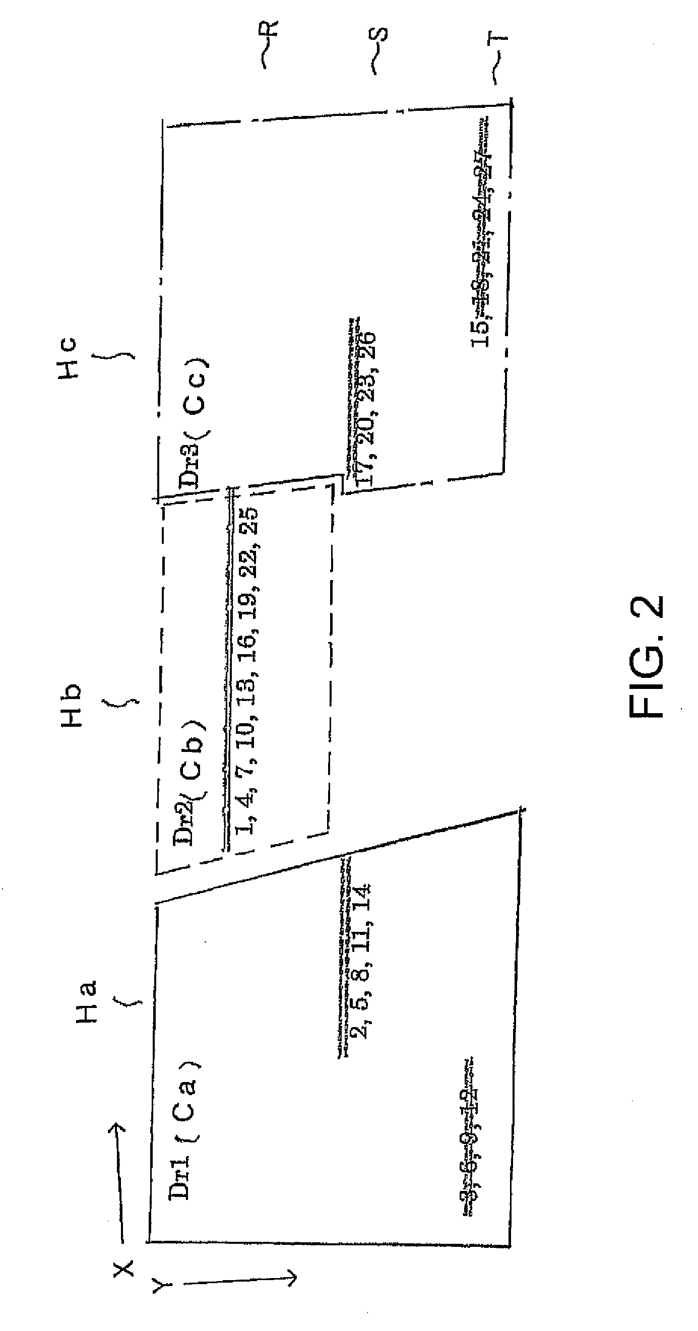
[0049]FIG. 3 is a schematic explanatory diagram showing an example of a line head according to an embodiment of the invention. In FIG. 3, A denotes an imaging lens with negative optical power, and B denotes a light emitting element group composed of a plurality of light emitting elements disposed inside the imaging lens A. The light emitting elements emit light towards the viewer of the sheet of FIG. 3. A plurality of imaging lenses A are disposed in the axial direction (the X or main-scanning direction) and in the rotational direction (the Y or sub-scanning direction) of the photoconductor drum. A plurality of light emitting element groups B disposed in the imaging lenses A is disposed in the X and Y directions in this example.

[0050]As described above, the imaging lenses A are arranged in the X and Y directions to form imaging lens rows R, S and T. The imaging lens rows also correspond to light emitting element rows. Therefore, light emitting element group rows R, S and T are forme...


PUM


Abstract

A line head includes a substrate, light emitting elements disposed on the substrate, drive circuits that drive the light emitting elements, and wirings that electrically connect the drive circuits and the light emitting elements. The light emitting elements form n (n≧2) light emitting element rows. The drive circuits are electrically connected with the wirings to light emitting elements belonging to a number of light emitting element rows equal to or smaller than n−1.

Description

CROSS-REFERENCE TO RELATED APPLICATIONS[0001]This application claims the benefit of priority under 35 USC 119 of Japanese patent application no. 2008-007832, filed on Jan. 17, 2008, and Japanese patent application no. 2008-208367, filed on Aug. 13, 2008, which are incorporated herein by reference.BACKGROUND[0002]1. Technical Field[0003]The present invention relates to a line head and an image forming device using the line head that simplify wiring connections where light sources are arranged two-dimensionally to be connected to a drive circuit, and that rationally perform image formation.[0004]2. Related Art[0005]A toner image formation section of an electrophotographic system generally includes a photoconductor drum as an image carrier having a photoconductive layer on its outer circumferential surface, a charging section for evenly charging the outer circumferential surface of the photoconductor drum, an exposure section for selectively exposing the outer circumferential surface t...

Claims


Application Information

Patent Timeline
IPC IPC(8): B41J2/435
CPCB41J2/155B41J2/451B41J2/45
Inventor TOGUCHI, TAKEHARU
Owner SEIKO EPSON CORP
Why Eureka
Try Eureka