Photoelectric amplification integrated triode chip

A photoelectric amplification and photodiode technology, applied in electrical components, electronic switches, pulse technology, etc., can solve the problems of magnification that changes with ambient temperature, inability to take into account signal-to-noise ratio and bandwidth, and difficulty in processing circuits, and achieves transmission response speed. Fast, miniaturized, and high signal-to-noise ratio

Pending Publication Date: 2021-07-13
GLOBAL ENERGY INTERCONNECTION RES INST CO LTD +2
View PDF0 Cites 0 Cited by
  • Summary
  • Abstract
  • Description
  • Claims
  • Application Information

AI Technical Summary

Problems solved by technology

When the light energy is weak, such as about 0.1 ~ 10μW, the corresponding photocurrent is relatively weak, which brings difficulty to the processing circuit of the subsequent stage, and cannot take into account the signal-to-noise ratio and bandwidth
[0003] Existing photodetector devices with current amplification function mainl

Method used


Image

  • Photoelectric amplification integrated triode chip
  • Photoelectric amplification integrated triode chip
  • Photoelectric amplification integrated triode chip

Examples


Embodiment 1

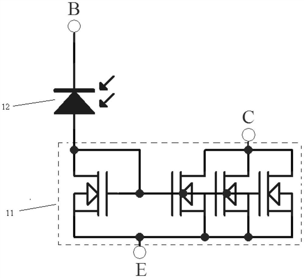
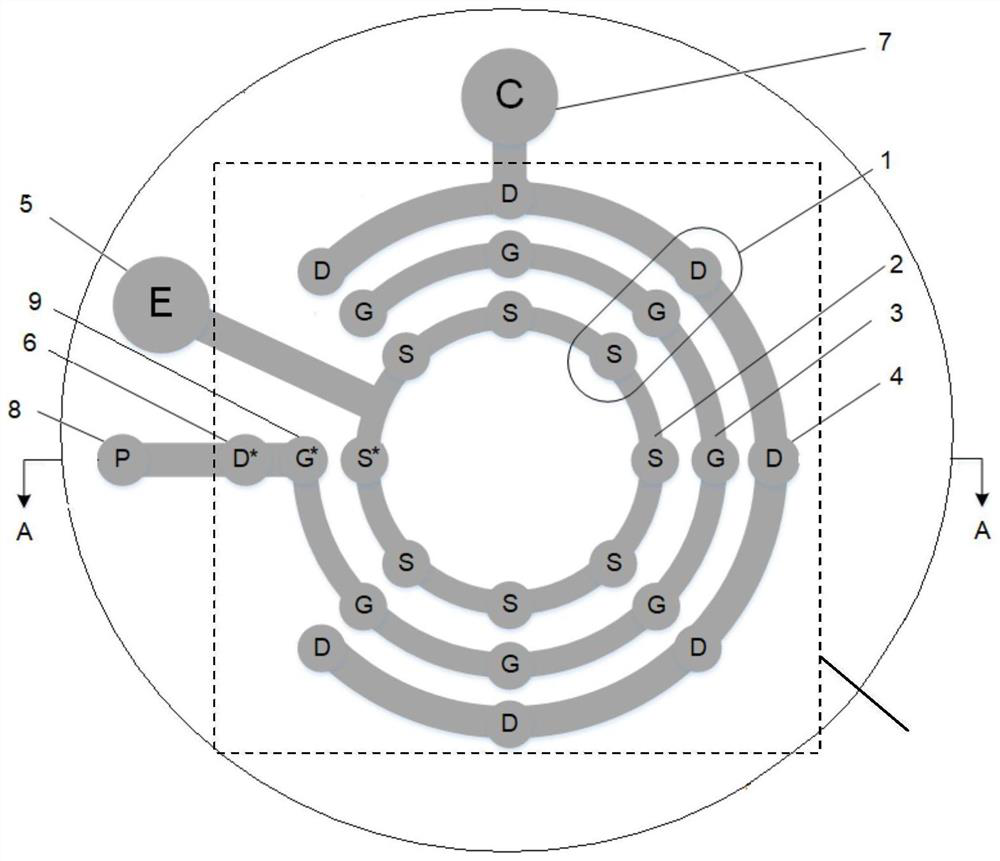
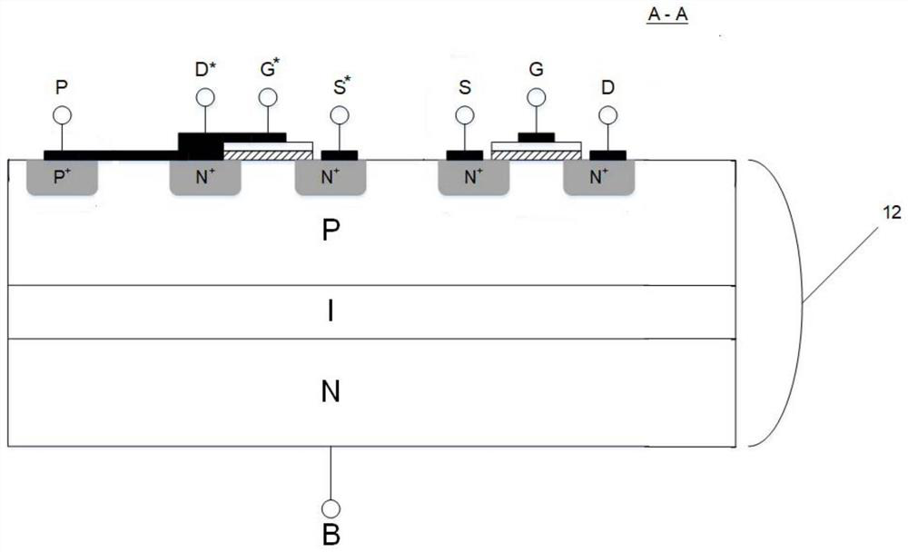
[0039] refer to figure 2 and image 3 , this embodiment provides a photoelectric amplification integrated triode chip, including:

[0040] The photodiode unit 12, the photodiode unit 12 includes a photodiode, and the photodiode is a PIN structure. Wherein the N-type layer is N-InP, the I layer is I-InGaAsP, and the P-type layer is P-InP.

[0041] In some other embodiments, the photodiode may also be a PN structure, or a photodiode with other structures.

[0042] The proportional current mirror unit 11. The proportional current mirror unit 11 uses the P-type layer of the photodiode unit 12 as a substrate and is electrically connected to the P-type layer of the photodiode. In some other embodiments, the proportional current mirror unit 11 may use the N-type layer of the photodiode unit 12 as a substrate and be electrically connected to the N-type layer of the photodiode.

[0043] The photoelectric amplification integrated triode chip of this embodiment realizes the amplific...

Embodiment 2

[0065] This embodiment provides a photoelectric amplifier integrated triode chip, which differs from the above-mentioned embodiment 1 in that:

[0066] The proportional current mirror unit includes a plurality of triodes, and the plurality of triodes include a receiving triode and a plurality of amplifying transistors;

[0067] The collector and the base of the receiving triode are electrically connected; the N-type layer or the P-type layer where the photodiode is electrically connected to the receiving triode is provided with a first heavily doped region and a plurality of second heavily doped regions, and the first heavily doped The conductivity type of the region is the same as that of the layer, the conductivity type of the plurality of second heavily doped regions is opposite to the conductivity type of the layer, and the plurality of second heavily doped regions are respectively located at positions corresponding to the collector and emitter of each triode; The first he...


PUM


Abstract

The invention discloses a photoelectric amplification integrated triode chip, comprising a photodiode unit, which comprises a photodiode, and the photodiode comprises a PIN structure photodiode or a PN structure photodiode; a proportional current mirror unit which takes the P-type layer or the N-type layer of the photodiode unit as a substrate, whherein the photodiode unit is electrically connected with the proportional current mirror unit. According to the scheme, amplification of the light current of the photodiode unit is achieved through the proportional current mirror unit, current amplification with stable temperature can be achieved, extra current noise is not introduced, the signal-to-noise ratio is not reduced, and the high signal-to-noise ratio is maintained.

Description

technical field [0001] The invention relates to the field of photoelectric chips, in particular to a photoelectric amplification integrated triode chip. Background technique [0002] Existing photon-type photodetectors are based on semiconductor chips with PN structure or PIN structure, which can convert light signals into current signals, and the maximum conversion rate is 1 photon corresponding to 1 electron. For example, the theoretical responsivity corresponding to 1550nm light wave is 1.25A / W. When the light energy is weak, such as about 0.1-10μW, the corresponding photocurrent is relatively weak, which brings difficulty to the processing circuit of the subsequent stage, and cannot take into account the signal-to-noise ratio and bandwidth. [0003] Existing photodetector devices with current amplification function mainly include APD based on avalanche effect and phototransistor based on triode effect, but they have two problems: one is that additional current noise is...

Claims


Application Information

Patent Timeline
IPC IPC(8): H03K17/687
CPCH03K17/687
Inventor 陈硕牛晓晨黄杰刘占元
Owner GLOBAL ENERGY INTERCONNECTION RES INST CO LTD
Why Eureka
Try Eureka