Supercharge Your Innovation With Domain-Expert AI Agents!

Transistor, method of manufacturing transistor, and method of operating transistor

a transistor and manufacturing method technology, applied in the field of semiconductor devices, can solve the problems of difficult high current supply and large heat generation of conventional fets, and achieve the effect of less heat and higher curren

Inactive Publication Date: 2009-07-23
SAMSUNG ELECTRONICS CO LTD
View PDF0 Cites 5 Cited by
  • Summary
  • Abstract
  • Description
  • Claims
  • Application Information

AI Technical Summary

Benefits of technology

The transistor generates less heat and provides higher current by controlling the phase change layer's conductivity with lower operating voltages, effectively managing the ON-state and OFF-state transitions.

Problems solved by technology

A conventional FET as described above may generate large quantity of heat because the conventional FET is operated by a comparative high operating voltage.
Accordingly, it may be difficult to supply high current.

Method used


Image

  • Transistor, method of manufacturing transistor, and method of operating transistor
  • Transistor, method of manufacturing transistor, and method of operating transistor
  • Transistor, method of manufacturing transistor, and method of operating transistor

Examples


Embodiment Construction

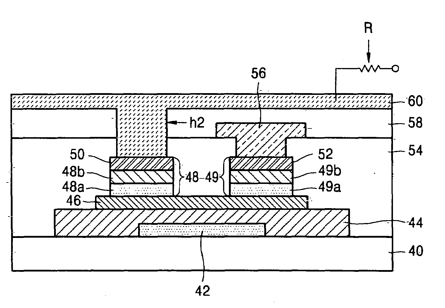
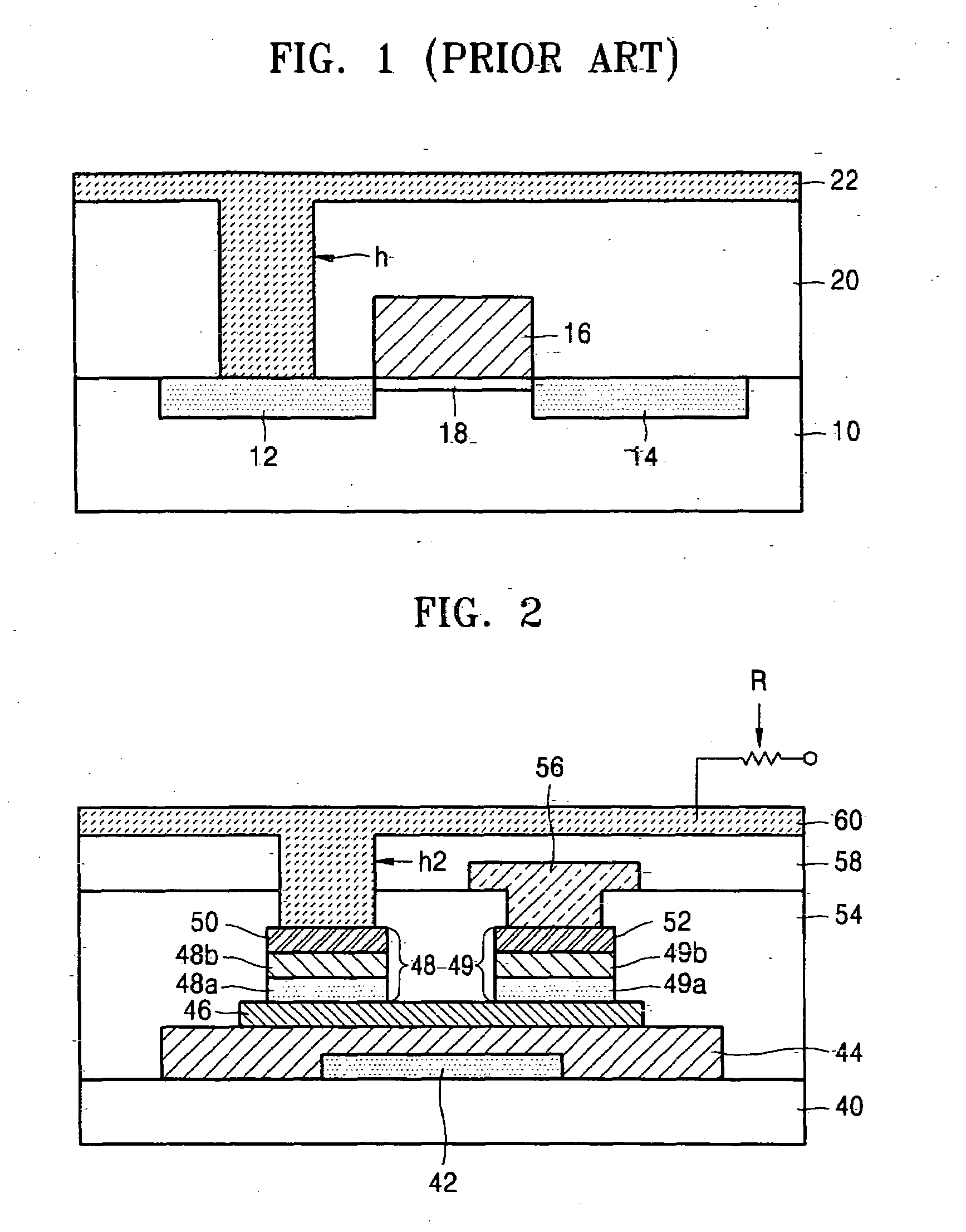
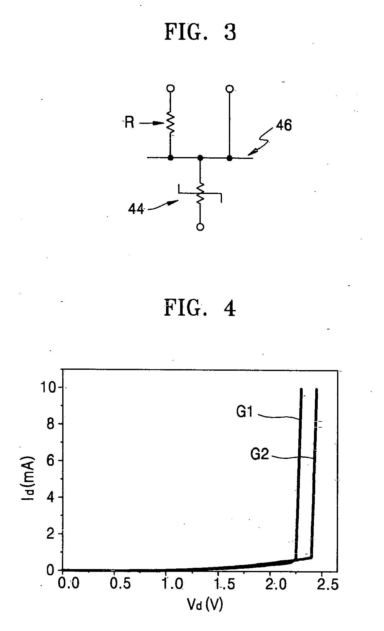
[0034]A transistor and a method of manufacturing and operating the same according to the present invention will now be described more fully with reference to the accompanying drawings, in which example embodiments of the invention are shown. In the drawings, the thicknesses of layers and regions are exaggerated for clarity.

[0035]Various example embodiments of the present invention will now be described more fully with reference to the accompanying drawings in which some example embodiments of the invention are shown. In the drawings, the thicknesses of layers and regions are exaggerated for clarity.

[0036]Detailed illustrative embodiments of the present invention are disclosed herein. However, specific structural and functional details disclosed herein are merely representative for purposes of describing example embodiments of the present invention. This invention may, however, may be embodied in many alternate forms and should not be construed as limited to only the embodiments set ...


PUM


Abstract

A transistor in which a physical property of its channel is changed according to an applied voltage, and methods of manufacturing and operating the same are provided. The transistor may include a first conductive layer on a substrate, a phase change layer and a second conductive layer which are sequentially stacked on the first conductive layer, a first current direction limiting unit and a second current direction limiting unit formed on the second conductive layer by being separated within a space, a third conductive layer and a fourth conductive layer formed on the first current direction limiting unit and the second current direction limiting unit, respectively, a word line connected to the third conductive layer, a bit line connected to the fourth conductive layer, and a voltage lowering unit connected to the word line.

Description

PRIORITY STATEMENT[0001]This application claims the benefit of Korean Patent Application No. 10-2004-0093639, filed on Nov. 16, 2004, in the Korean Intellectual Property Office, the disclosure of which is incorporated herein in its entirety by reference.BACKGROUND OF THE INVENTION[0002]1. Field of the Invention[0003]Example embodiments of the present invention relate to a semiconductor device and a method of manufacturing the same, and more particularly, to a transistor, a method of manufacturing a transistor, and method of operating a transistor.[0004]2. Description of the Related Art[0005]Transistors used in a semiconductor device may be field effect transistors (FET). An FET may maintain a signal transmission path as an ON-state or an OFF-state according to an applied voltage in a semiconductor device.[0006]FIG. 1 illustrates a conventional field effect transistor (FET).[0007]Referring to FIG. 1, a semiconductor substrate 10 may include a source region 12 and a drain region 14. T...

Claims


Application Information

Patent Timeline
Patent Type & Authority Applications(United States)
IPC IPC(8): H01L21/20H10B99/00
CPCH01L29/685H01L21/18
Inventor CHO, CHOONG-RAEYOO, IN-KYEONGLEE, MYOUNG-JAE
Owner SAMSUNG ELECTRONICS CO LTD
Features
  • R&D
  • Intellectual Property
  • Life Sciences
  • Materials
  • Tech Scout
  • Unparalleled Data Quality
  • Higher Quality Content
  • 60% Fewer Hallucinations
Learn More