Flexible Multilayer Printed Circuit Assembly with Reduced EMI Emissions
- Summary
- Abstract
- Description
- Claims
- Application Information
AI Technical Summary
Benefits of technology
Problems solved by technology
Method used
Image
Examples
Embodiment Construction
[0027]The invention will now be described in more detail by way of example with reference to the embodiments shown in the accompanying figures. It should be kept in mind that the following described embodiments are only presented by way of example and should not be construed as limiting the inventive concept to any particular physical configuration.
[0028]Further, if used and unless otherwise stated, the terms “upper”, “lower”, “front”, “back”, “over”, “under”, and similar such terms are not to be construed as limiting the invention to a particular orientation. Instead, these terms are used only on a relative basis.
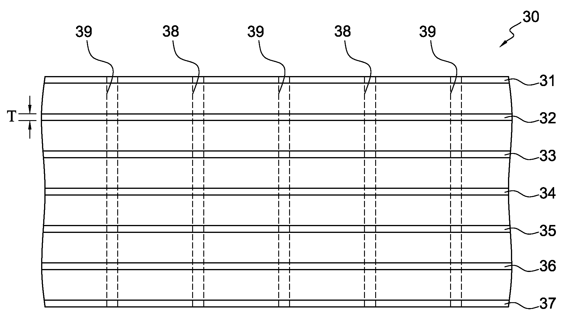
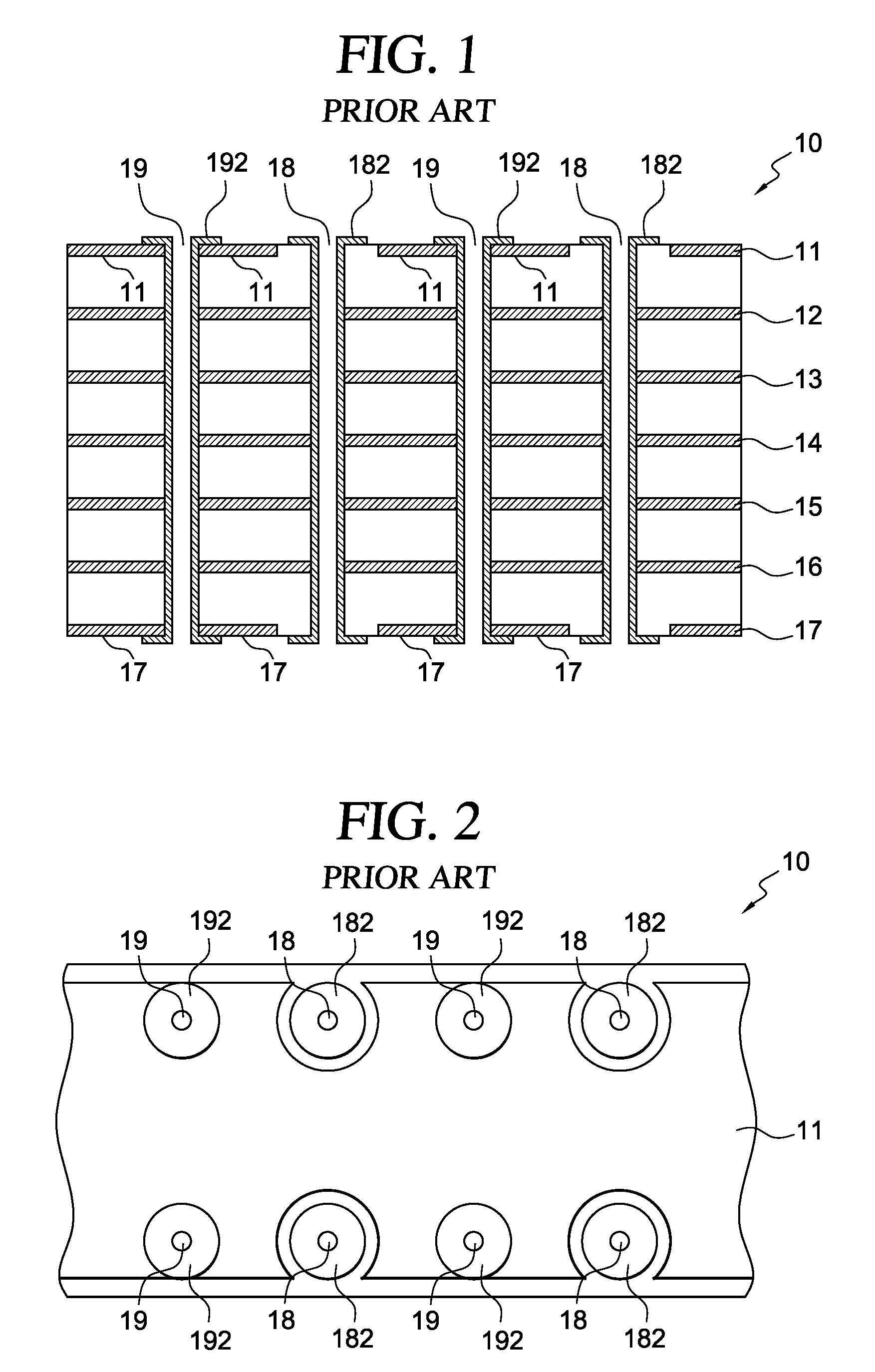
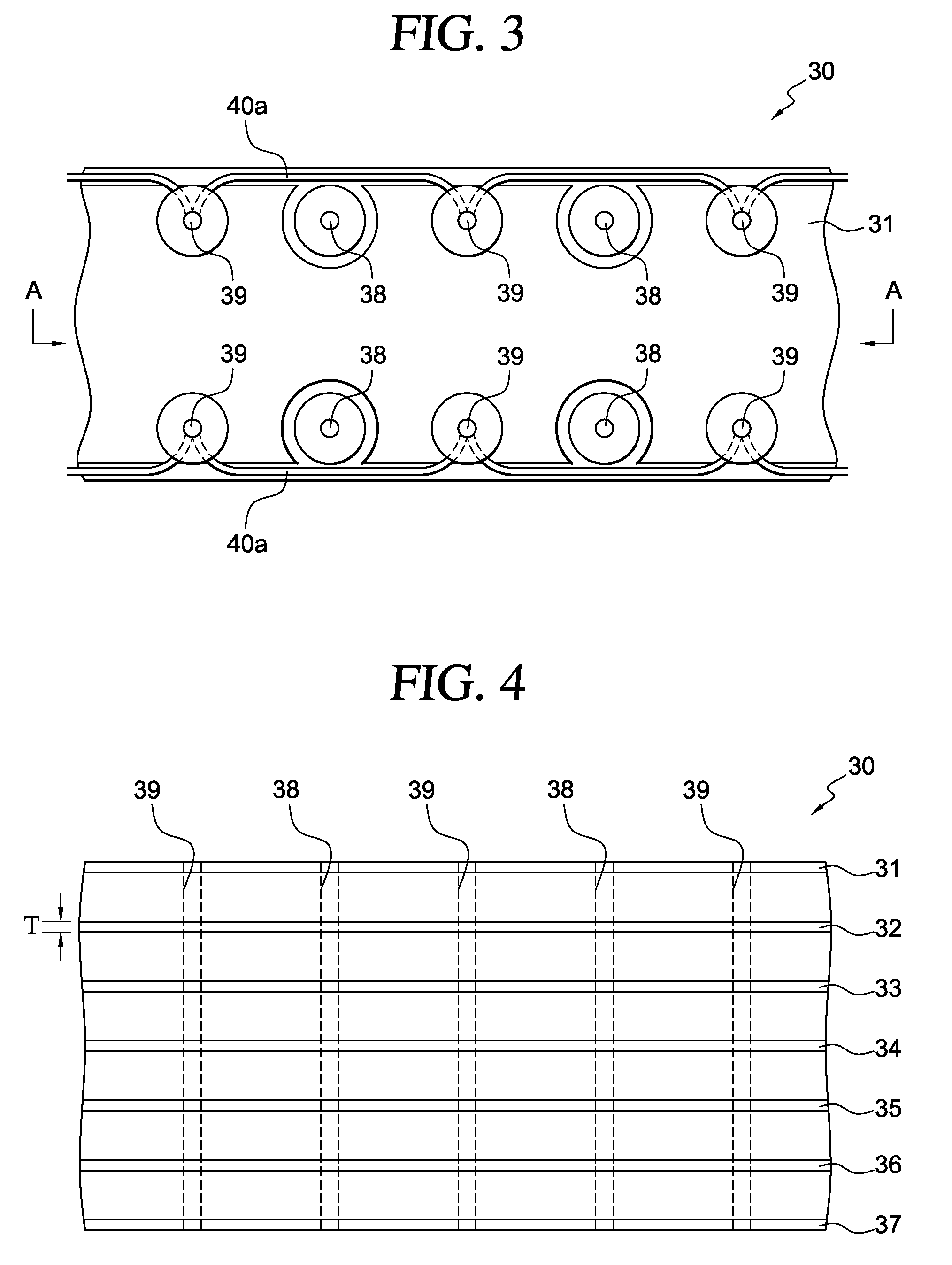
[0029]FIG. 3 is a partial top plan view of a flexible multilayer printed circuit assembly 30, according to an exemplary embodiment of the invention. The printed circuit assembly 30 includes multiple conductive layers that are made of conductive material. The multiple conductive layers may have similar layer structure of the assembly 10, as shown in FIG. 1. Referring to FIG...
PUM
| Property | Measurement | Unit |
|---|---|---|
| Thickness | aaaaa | aaaaa |
| Flexibility | aaaaa | aaaaa |
| Height | aaaaa | aaaaa |
Abstract
Description
Claims
Application Information


