

Ultra-thin body super-steep retrograde well (SSRW) FET devices
- Summary
- Abstract
- Description
- Claims
- Application Information
AI Technical Summary
Benefits of technology
Problems solved by technology
Method used
Image

Examples
example i
[0056] In this example, two Silicon-On-Insulator (SOI) substrates, each having an SOI layer that has a thickness of about 55 nm were employed. Each of the SOI substrates, in particular each SOI layer, was doped with boron (B) by ion implantation using an ion dose of 2E13 B atoms / cm implanted at an energy of 10 keV in an ion implanter tool. The samples were then annealed at about 1000° C. for less than 10 seconds. Each SOI substrate was then subjected to a step in which the SOI layer was hydrogen terminated. The hydrogen termination was provided by applying dilute hydrofluoric acid to each of the SOI substrates at room temperature. After hydrogen termination, one of the SOI substrates was soaked at room temperature in a solution of 5×10⁻⁴ M iodine in methanol to provide a methoxy termination comprising carbon and oxygen bonded to the SOI layer as a monolayer of Si—O—CH 3. The iodine / methanol soak occurred at room temperature for about 20 minutes. The soaked SOI substrate was then rin...
example ii
[0057] Another SOI substrate was processed using the iodine / methanol treatment method of the present invention described above and thereafter the sample was annealed in vacuum at 850° C. and then an epitaxial Si overlayer having a thickness of about 30 nm was deposited at 850° C. A high-resolution (3 nm scale) TEM image and low resolution (50 nm scale) TEM of this sample were made. The TEMs illustrate that the iodine / methanol treatment step of the present invention does not disrupt the epitaxial alignment of the Si overlayer on the lattice structure of the original SOI layer. The carbon and oxygen doses for the interface between the SOI layer and the Si overlayer were 1.1E14 atoms / cm2 and 1.1E13 atoms / cm2, respectively. The interface is not visible by TEM, and the lattice of the SOI substrate is not distinguishable from the epitaxial Si overlayer.
Form Intrinsic Epitaxial Layers Over SOI Regions
[0058]FIG. 3M shows the device 30 of FIG. 3L after formation of ultra-thin intrinsic ep...
first embodiment
of the Method of the Invention
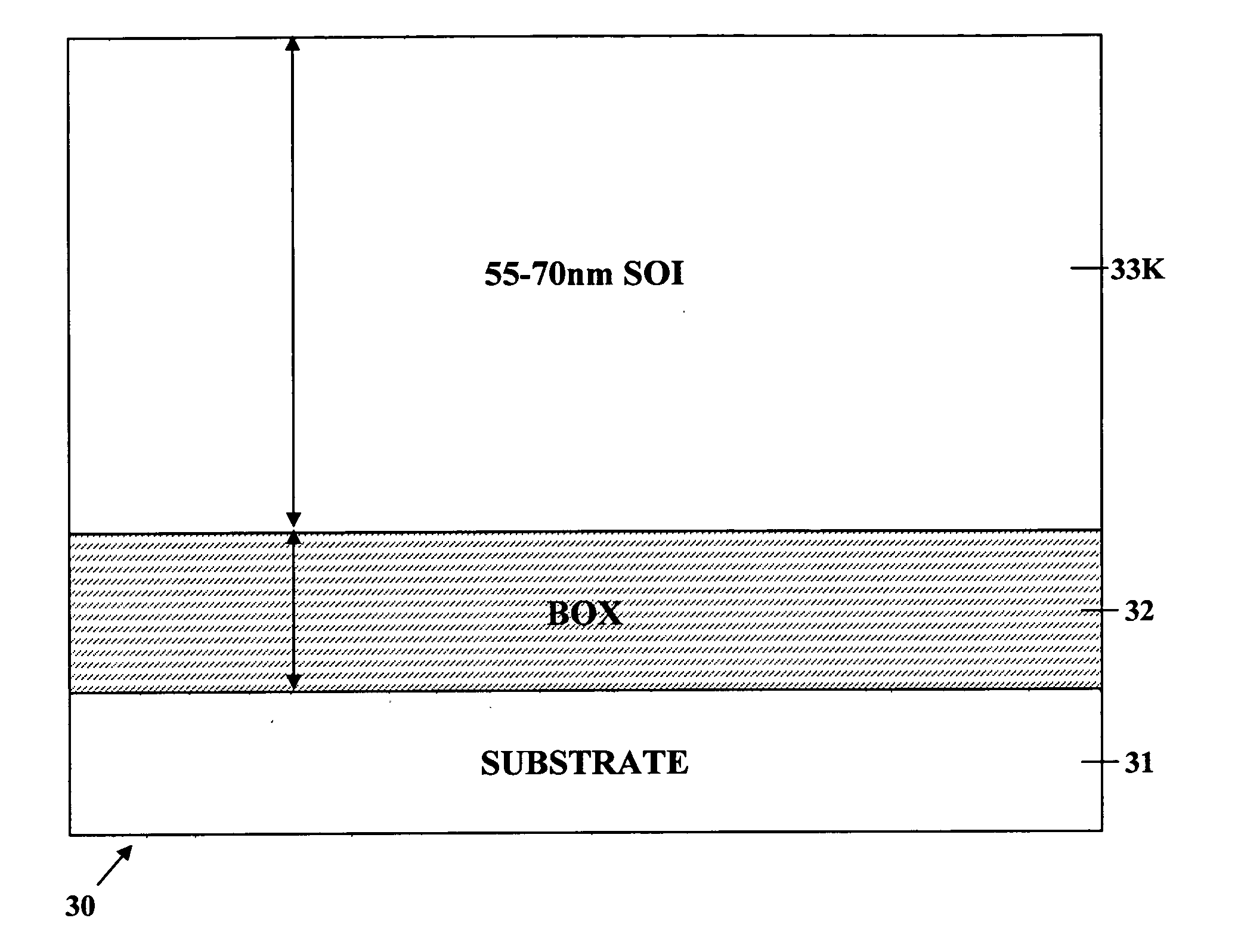
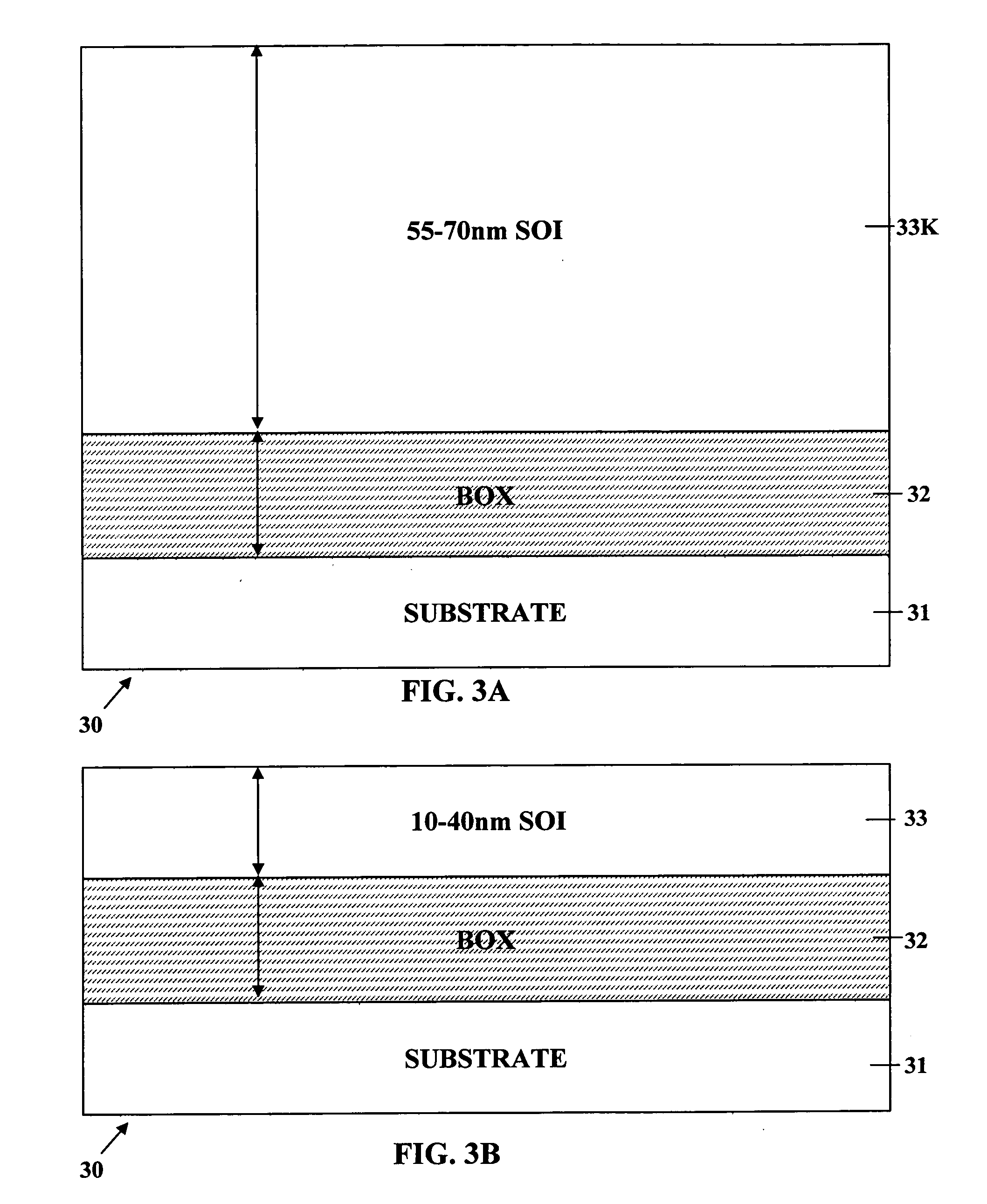
[0061]FIG. 4 shows a flow chart of a first embodiment of the method of this invention. The process illustrated by FIG. 4 begins at Start 70 and continues to step 71 in which device 30 is processed. The SOI layer 33K on BOX substrate 31 which initially had a thickness of 55 nm or more in FIG. 3A is thinned to an ultra-thin thickness from about 10 nm to about 40 nm by a process of oxidation and stripping as described above with reference to FIG. 3B.
[0062] At the end of step 71, the desired thickness of the SOI layer 33 has been reached.
[0063] In step 72, pad oxide layer 34, pad nitride layer 35 were formed as shown in FIG. 3C over the thinned SOI layer 33. Then, as shown in FIG. 3D, an isolation patterning mask 36L / 36R with a central isolation opening 36W therethrough was formed over the pad nitride layer 35 (above the SOI layer 33).
[0064] In step 73, an isolation trench 37 was formed by etching from the top of the device 30 down through the isolation ...
PUM
 Abstract
Description
Claims
Application Information