

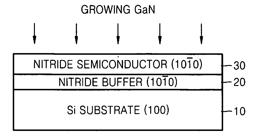
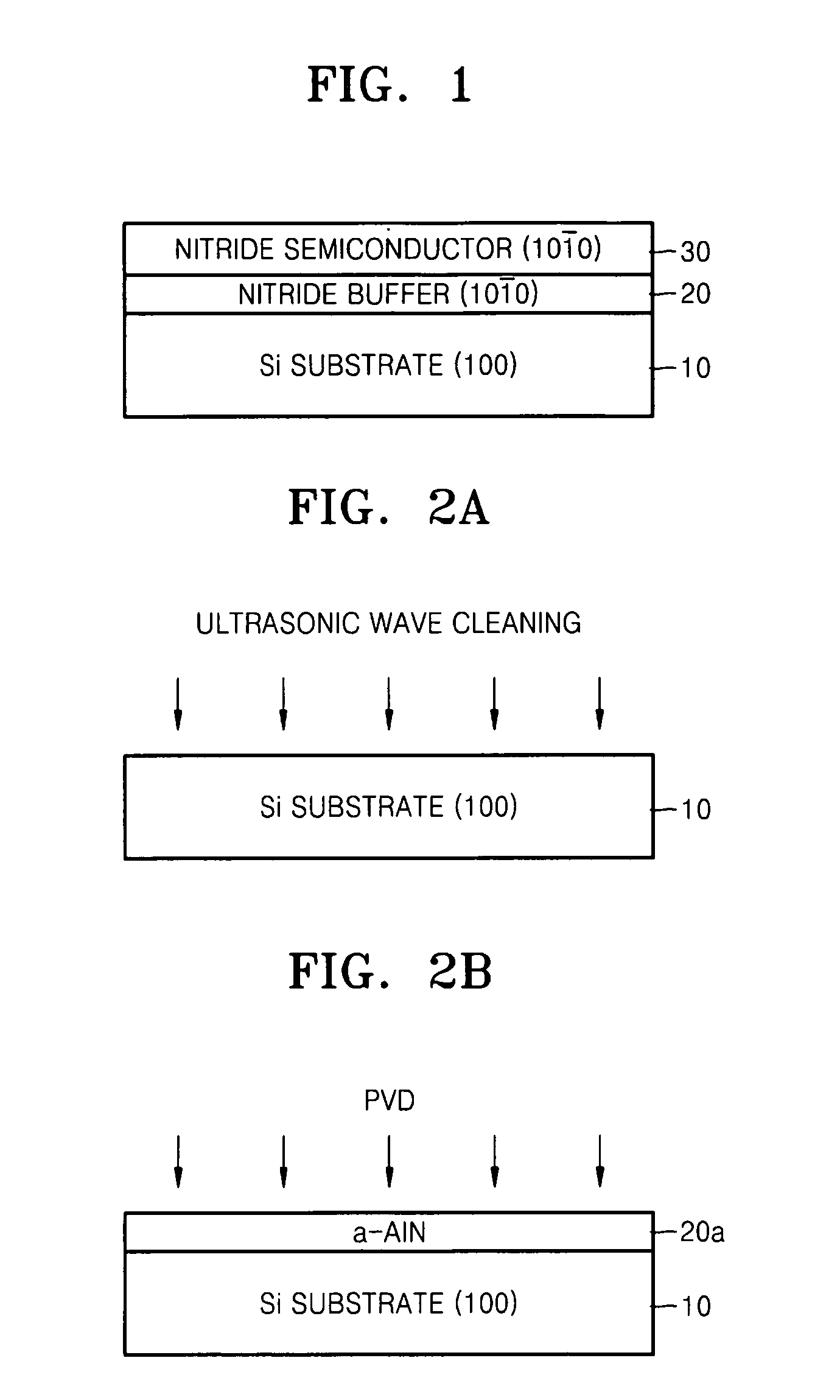
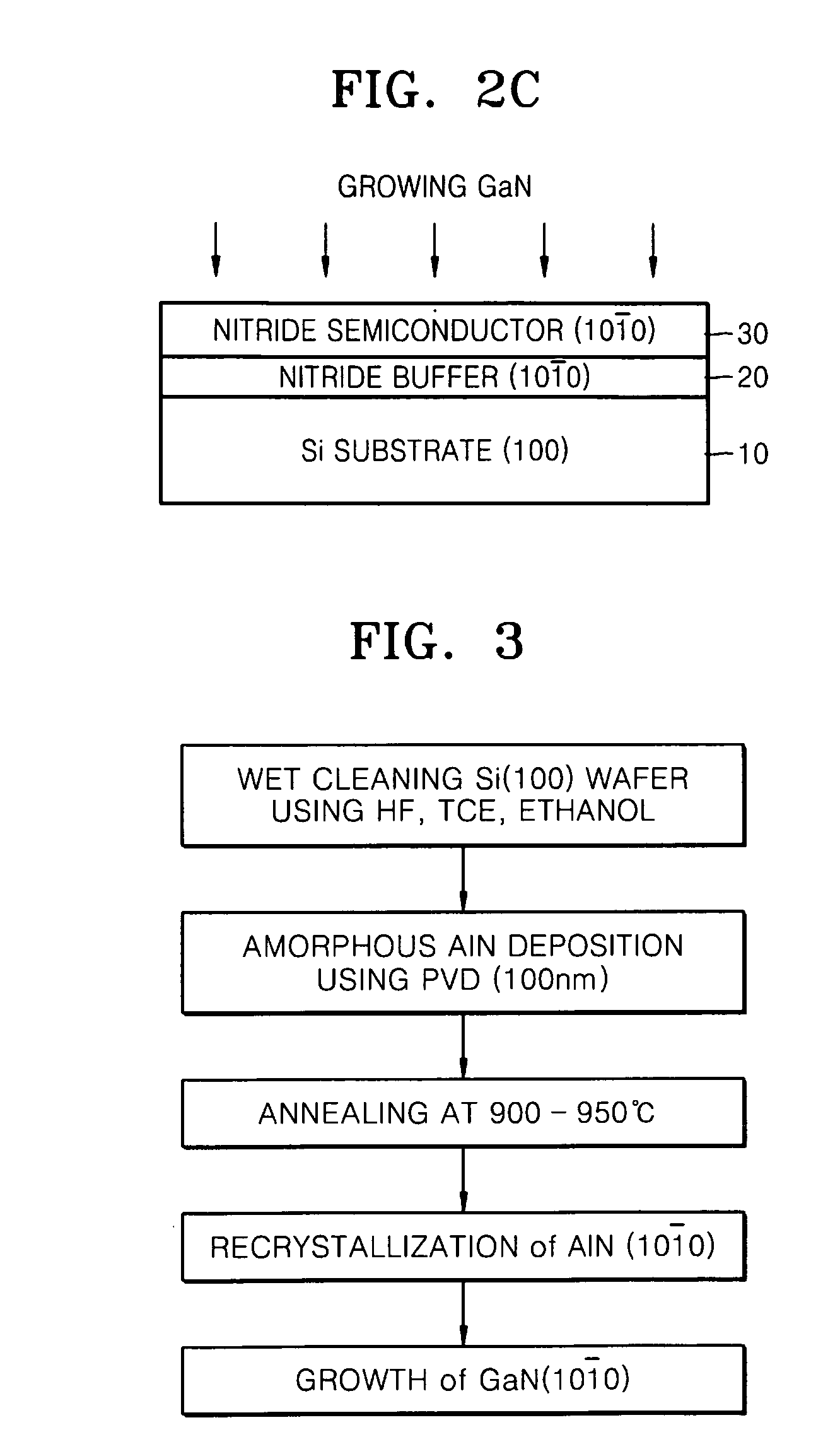
Method of manufacturing nitride semiconductor substrate
a manufacturing method and technology of nitride, applied in the direction of basic electric elements, electrical apparatus, semiconductor devices, etc., can solve the problems of relatively high cost of r-plane sapphire and defect generation, and achieve the effect of low cos
- Summary
- Abstract
- Description
- Claims
- Application Information
AI Technical Summary
Benefits of technology
Problems solved by technology
Method used
Image

Examples
Embodiment Construction
[0022]It will be understood that when an element or layer is referred to as being “on”, “connected to”, “coupled to”, or “covering” another element or layer, it may be directly on, connected to, coupled to, or covering the other element or layer or intervening elements or layers may be present. In contrast, when an element is referred to as being “directly on,”“directly connected to,” or “directly coupled to” another element or layer, there are no intervening elements or layers present. Like numbers refer to like elements throughout the specification. As used herein, the term “and / or” includes any and all combinations of one or more of the associated listed items.
[0023]It will be understood that, although the terms first, second, third, etc. may be used herein to describe various elements, components, regions, layers, and / or sections, these elements, components, regions, layers, and / or sections should not be limited by these terms. These terms are only used to distinguish one elemen...
PUM
| Property | Measurement | Unit |
|---|---|---|
| temperature | aaaaa | aaaaa |
| temperature | aaaaa | aaaaa |
| temperature | aaaaa | aaaaa |
Abstract
Description
Claims
Application Information