Semiconductor light receiving element and method of manufacturing semiconductor light receiving element, and optical communication system

Active Publication Date: 2009-08-06
SONY CORP
View PDF2 Cites 5 Cited by
  • Summary
  • Abstract
  • Description
  • Claims
  • Application Information

AI Technical Summary

Benefits of technology

[0018]In the semiconductor light receiving element and the method of manufacturing the semiconductor light receiving element, and the optical communication system according to an embodiment of the present invention, an oxidation layer including a non-oxidation region and an oxidation region in a stacking in-plane direction is provided in a light absorbing layer o

Problems solved by technology

Hei 1-239973, there is an issue that the capacity between the upper electrode and the lower electrode is not reduced and still large.
In Japanese Patent No. 3183931, there is an issue that, to sufficiently reduce the ca

Method used


Image

  • Semiconductor light receiving element and method of manufacturing semiconductor light receiving element, and optical communication system
  • Semiconductor light receiving element and method of manufacturing semiconductor light receiving element, and optical communication system
  • Semiconductor light receiving element and method of manufacturing semiconductor light receiving element, and optical communication system

Examples


Embodiment Construction

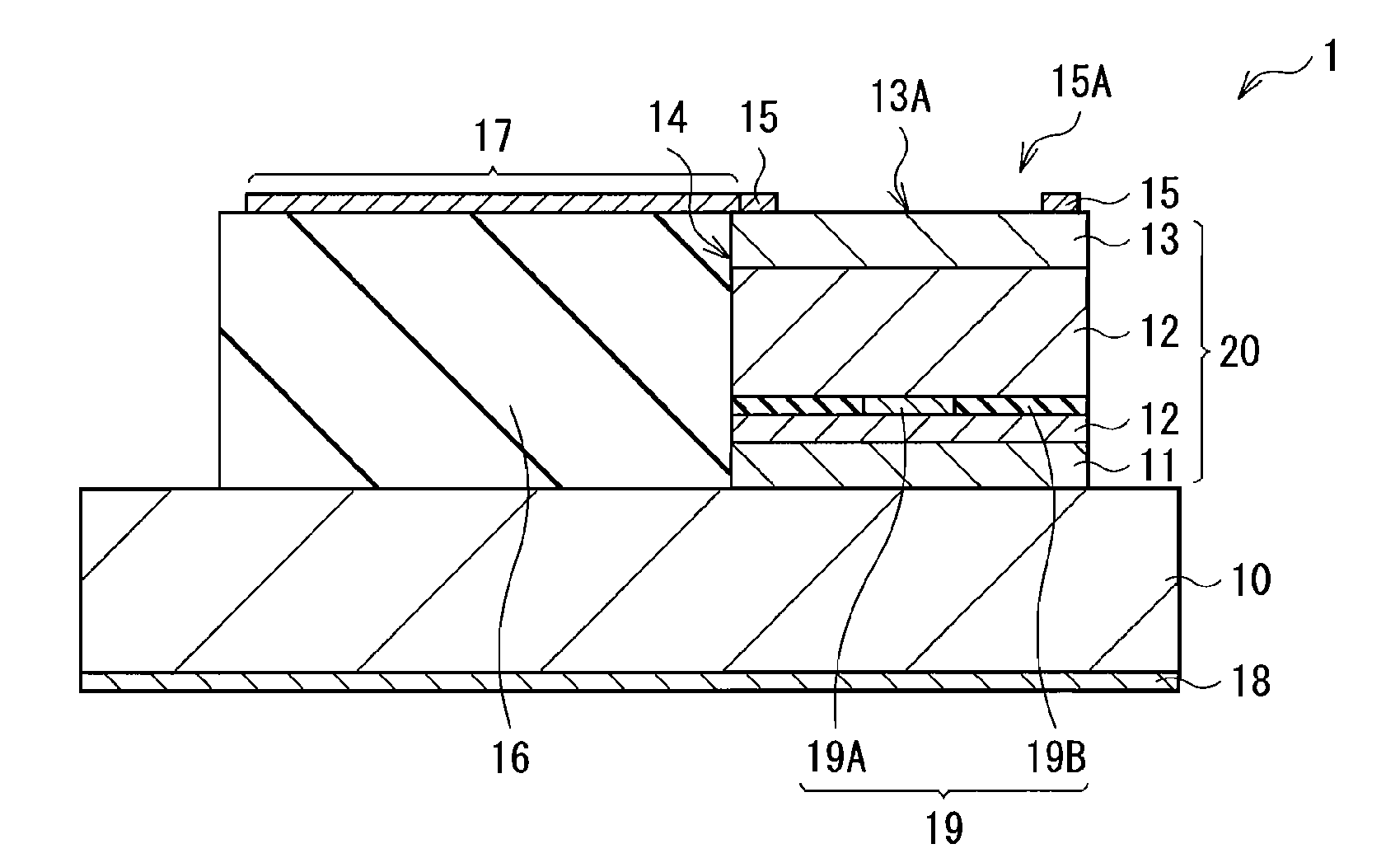
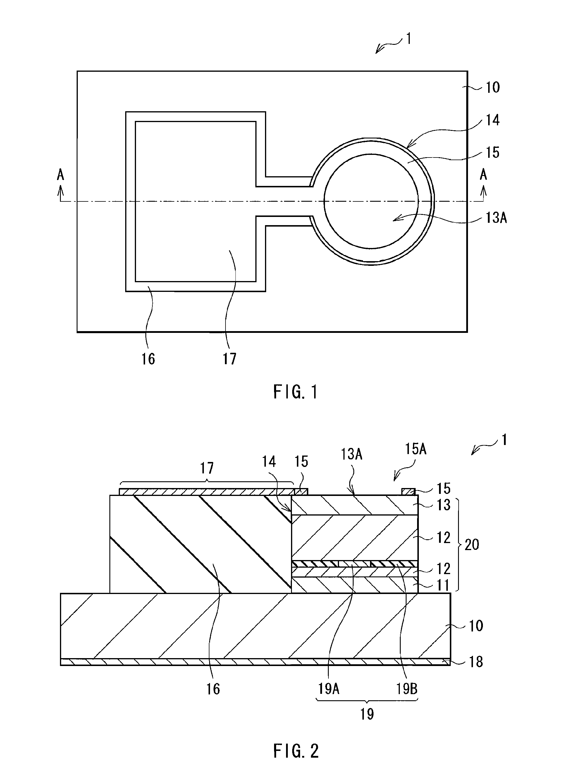
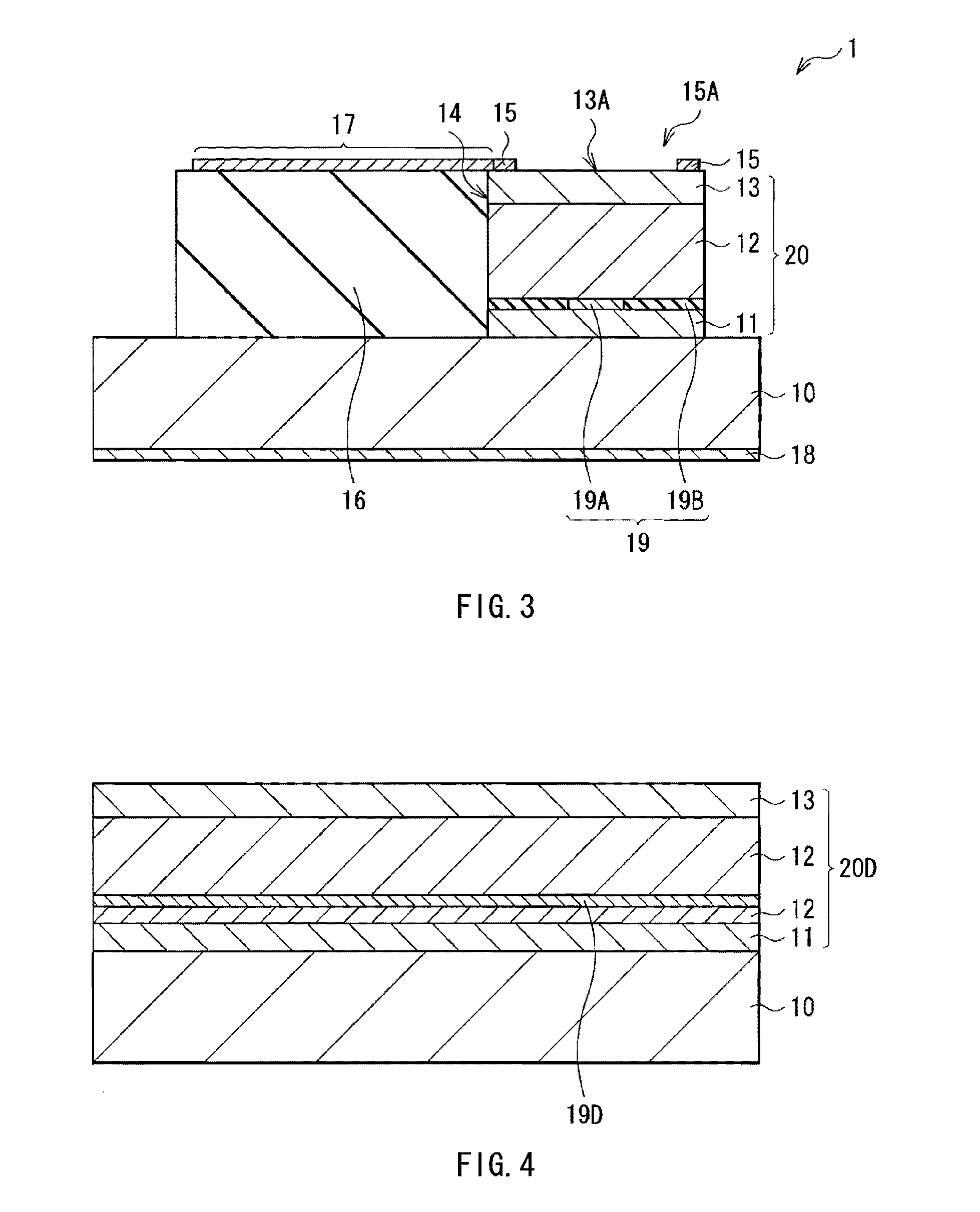
[0027]A preferred embodiment of the present invention will be described in detail with reference to the accompanying drawings.

[0028]FIG. 1 illustrates a top view of a surface-emitting semiconductor light receiving element 1 according to an embodiment of the present invention. FIGS. 2 and 3 illustrate examples of the cross-sectional configuration as viewed from the direction of arrow A-A of the semiconductor light receiving element 1 of FIG. 1, respectively. FIGS. 1 to 3 are schematic views with dimensions and shapes different from actual dimensions and actual shapes.

[0029]The semiconductor light receiving element 1 is suitably applicable to an optical communication system performing signal transmission (optical transmission) between semiconductor chips such as LSIs, and includes, on a semiconductor substrate 10, a stacked structure 20 including a first conductivity type layer 11, a light absorbing layer 12, and a second conductivity type layer 13 in this order from the semiconductor...


PUM


Abstract

The present invention provides a semiconductor light receiving element capable of reducing capacity while minimizing increase in travel time of carriers. The semiconductor light receiving element includes a semiconductor stacked structure including a first conductivity type layer, a light absorbing layer, and a second conductivity type layer having a light incidence plane in order. The semiconductor light receiving element has an oxidation layer including a non-oxidation region and an oxidation region in a stacking in-plane direction in the light absorbing layer or between the first conductivity type layer and the light absorbing layer.

Description

CROSS REFERENCES TO RELATED APPLICATIONS[0001]The present invention contains subject matter related to Japanese Patent Application JP 2008-026355 filed in the Japanese Patent Office on Feb. 6, 2008, the entire contents of which being incorporated herein by reference.BACKGROUND OF THE INVENTION[0002]1. Field of the Invention[0003]The present invention relates to a semiconductor light receiving element suitably applicable to optical communication and a method of manufacturing the same, and an optical communication system including the semiconductor light receiving element.[0004]2. Description of the Related Art[0005]In general, in a PIN photodiode (p-intrinsic-n photodiode) for optical communication, a columnar mesa is formed by stacking an n-type buffer layer, a light absorbing layer, and a p-type cap layer on an n-type semiconductor substrate, for example, as described in Japanese Unexamined Patent Publication No. Hei 1-239973. On the upper surface of the mesa, a ring-shaped upper e...

Claims


Application Information

Patent Timeline
IPC IPC(8): H01L31/0352H01L31/18
CPCG02B6/42H01L31/1055G02B6/4246G02B6/4206
Inventor YAMAUCHI, YOSHINORIARAKIDA, TAKAHIROKODA, RINTAROYAMAGUCHI, NORIHIKOMASUI, YUJIOKI, TOMOYUKI
Owner SONY CORP
Why Eureka
Try Eureka