Display device and method of manufacturing display device

Active Publication Date: 2009-08-13
JOLED INC
View PDF0 Cites 27 Cited by
  • Summary
  • Abstract
  • Description
  • Claims
  • Application Information

AI Technical Summary

Benefits of technology

[0013]As described above, according to the present invention, by providing the multiple pieces of annular wiring, a short-circuit part between the lead wiring and the annular wiring disposed above the lead wiring can be easily

Problems solved by technology

In such a constitution, a short circuit tends to occur due to foreign matter or a pattern abno

Method used


Image

  • Display device and method of manufacturing display device
  • Display device and method of manufacturing display device
  • Display device and method of manufacturing display device

Examples


Embodiment Construction

[0028]A preferred embodiment of the present invention will hereinafter be described in detail with reference to the drawings. Incidentally, in the embodiments, description will be made of a general constitution of a display device, a pixel circuit on a lower layer side close to a substrate, a constitution of a light emitting element disposed above the pixel circuit, and a method of manufacturing the display device in this order.

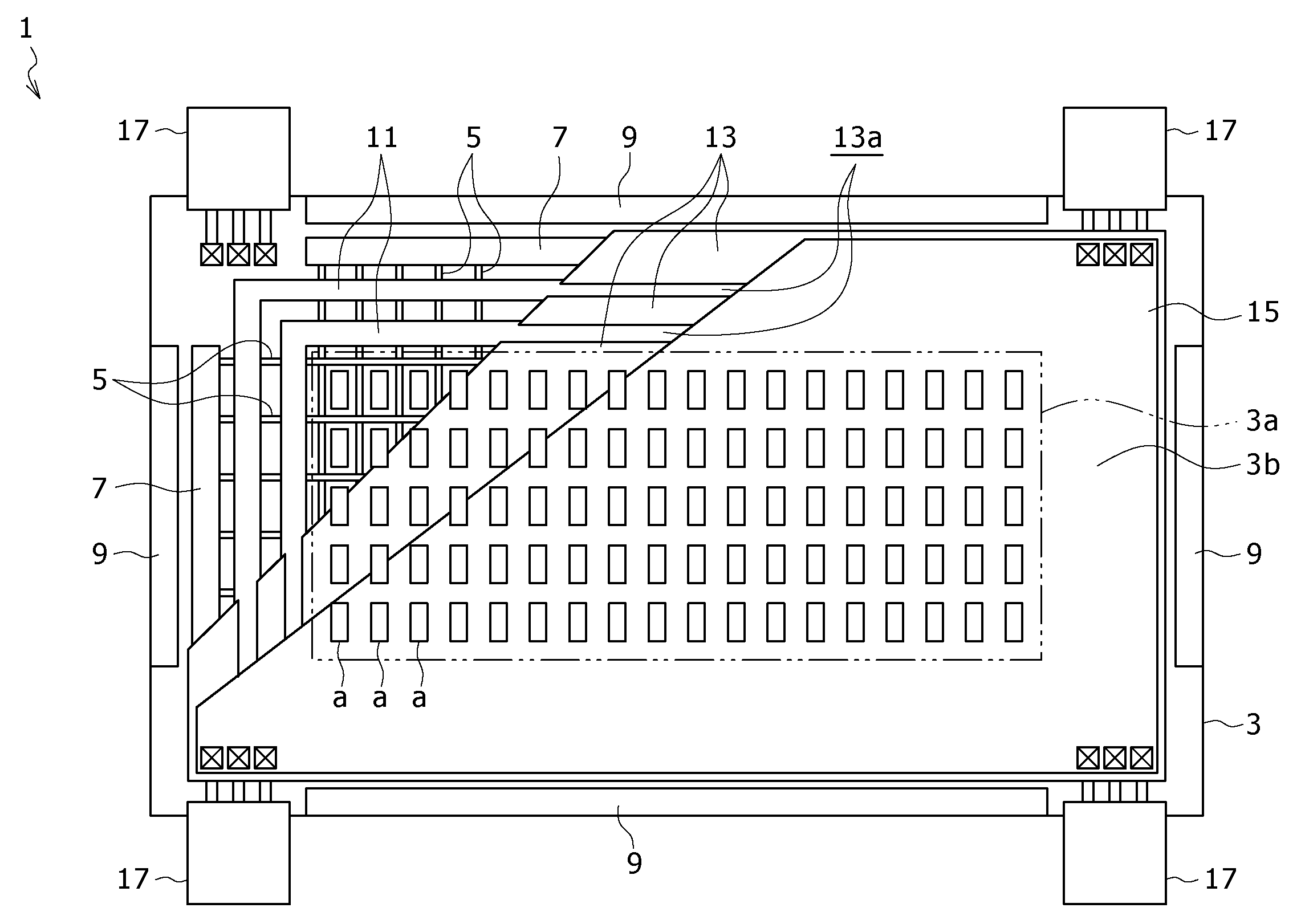
[0029]FIG. 1 is a layout diagram showing a general constitution of a display device 1 according to an embodiment, and is a plan view with a part of constituent elements cut away. The display device 1 shown in this figure is an organic EL display device formed by arranging organic electroluminescent light emitting elements EL, and is an active matrix driving display device in which each organic electroluminescent light emitting element EL is connected with a driving circuit.

[0030]As shown in this figure, a display region 3a having a substantially rectangular p...


PUM


Abstract

A display device includes lead wiring drawn out from a display region to a peripheral region of the display region; a first insulating film covering the lead wiring disposed on a substrate; a plurality of pieces of annular wiring disposed in a state of enclosing the display region in a multiple manner between the display region and the peripheral region on the first insulating film; a second insulating film covering the annular wiring disposed above the substrate, and having a groove pattern having each of the pieces of annular wiring as a bottom surface; and a light emitting element disposed on the second insulating film within the display region.

Description

CROSS REFERENCES TO RELATED APPLICATIONS[0001]The present invention contains subject matter related to Japanese Patent Application JP 2008-031559, filed in the Japan Patent Office on Feb. 13, 2008, the entire contents of which being incorporated herein by reference.BACKGROUND OF THE INVENTION[0002]1. Field of the Invention[0003]The present invention relates to a display device and a method of manufacturing the display device, and particularly to a display device that can be repaired easily and which provides a high margin for a manufacturing process, and a method of manufacturing the display device.[0004]2. Description of the Related Art[0005]An organic electroluminescent light emitting element (so-called organic EL element) using the electroluminescence (hereinafter described as EL) of an organic material is formed by disposing an organic layer between two electrodes, the organic layer being formed by laminating an organic hole transporting layer and an organic light emitting layer...

Claims


Application Information

Patent Timeline
IPC IPC(8): H01J1/53H01J9/20
CPCH01L27/3258H01L2251/568H01L51/5228H01L27/3276H10K59/124H10K59/131H10K50/824H10K71/861
Inventor SAGAWA, HIROSHIUCHINO, KATSUHIDE
Owner JOLED INC
Why Eureka
Try Eureka