Imager wafer level module and method of fabrication and use

a technology of imager wafers and modules, applied in the field of digital imaging, can solve problems such as production costs

Inactive Publication Date: 2009-08-20
APTINA IMAGING CORP
View PDF21 Cites 99 Cited by
  • Summary
  • Abstract
  • Description
  • Claims
  • Application Information

AI Technical Summary

Problems solved by technology

One problem experienced in realizing the low production costs and high yields of CMOS imager senso

Method used


Image

  • Imager wafer level module and method of fabrication and use
  • Imager wafer level module and method of fabrication and use
  • Imager wafer level module and method of fabrication and use

Examples


first embodiment

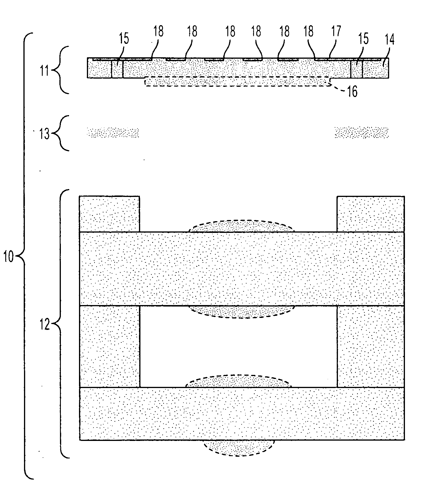
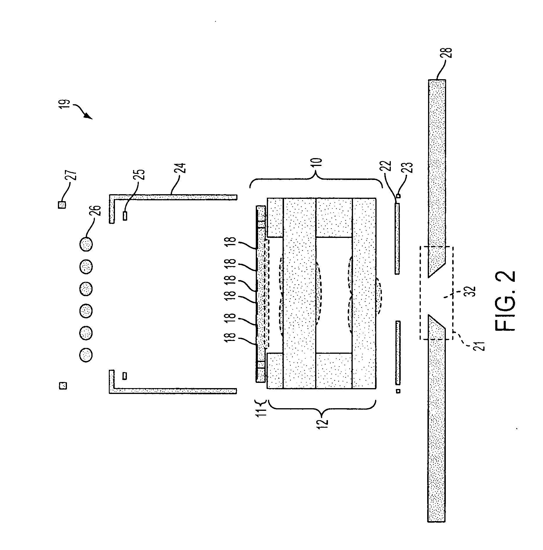
[0033]Once a plurality of imager wafer level modules 19 have been assembled on a molded plastic interposer 28, the plurality of imager wafer level modules 19 can be separated into individual imager wafer level modules 19, or groups of imager wafer level modules 19 as required for a specific application. This process of separation is known as singulation. FIG. 5 is an overhead view of a representative molded plastic interposer 28, with representative saw streets 33, which can be used by a saw to singulate individual imager wafer level modules 19 from a plurality of wafer level modules 19. For example, and not intended to be limiting, in FIG. 5 three module assemblies could be placed over the three apertures 32. As presented previously, these three module assemblies 10 could be assembled by either of two methods. In a first embodiment, module assemblies 10 could be assembled as individual module assemblies 10 and placed individually over their respective apertures 32 such that light w...

second embodiment

[0034]FIG. 3 is a cross-sectional expanded view of the components of a second embodiment imager wafer level module 19′ with a plastic laminate interposer 29. Elements in FIG. 3 referring to like elements in FIGS. 1-2A have the same reference numerals. In the illustrated embodiment, a light guide 31 may also be included. Whether or not an interposer light guide 21 is present with the required aperture 32, the imager wafer level module 19′ may also have light guide 31. This light guide 31, similar to the interposer light guide 21, is used to discriminate between light that should pass, and light that should not pass to the imager 16 (FIG. 1) of the module assembly 10.

[0035]FIG. 3A is a cross-sectional view of an assembled imager wafer level module 19′ with the plastic laminate interposer 29. The components within FIG. 3A are arranged identical to those found in FIG. 2A, with the addition of optional light guide 31 attached to the plastic laminate interposer 29.

[0036]Referring to FIGS....


PUM


Abstract

Imager wafer level modules, methods of assembly for imager wafer level modules, and systems containing imager wafer level modules. An imager die and an optic lens stack are combined to form a module assembly. The module assembly is combined with a molded plastic, laminated plastic, or metallic interposer to form an imager wafer level module capable of assembly using industry standard equipment sets for all processing, and capable of being used with various imaging systems.

Description

FIELD OF THE INVENTION[0001]The embodiments described herein relate generally to the field of digital imaging, and more specifically to imager wafer level modules, methods for assembling imager wafer level modules, and systems incorporating imager wafer level modules.BACKGROUND OF THE INVENTION[0002]Microelectronic imagers are used in digital cameras, wireless devices with picture capabilities, and many other applications. Cellular telephones and Personal Digital Assistants (PDAs), for example, are incorporating microelectronic imagers for capturing and sending pictures. The growth rate of microelectronic imagers has been steadily increasing as they become smaller and produce better images with higher pixel counts.[0003]Microelectronic imagers include image sensors that use Charged Coupled Device (CCD) systems, Complementary Metal-Oxide Semiconductor (CMOS) systems or other imager technology systems. CCD image sensors have been widely used in digital cameras and other applications. ...

Claims


Application Information

Patent Timeline
IPC IPC(8): H01L21/00H01L27/00
CPCG02B7/02H01L27/14618H01L27/14625H04N5/2257H01L31/0232H04N5/2253H04N5/2254H01L31/0203H01L2924/0002H01L27/14687H04N23/54H04N23/57H01L2924/00
Inventor BOLKEN, TODD O.VANAM, KIRAN
Owner APTINA IMAGING CORP
Why Eureka
Try Eureka