Liquid crystal display device
a liquid crystal display and display device technology, applied in semiconductor devices, optics, instruments, etc., can solve the problems of image sticking, cross-talk, flickering phenomenon, etc., to reduce the spacing distance, enhance the aperture ratio, and reduce the length of common lines
- Summary
- Abstract
- Description
- Claims
- Application Information
AI Technical Summary
Benefits of technology
Problems solved by technology
Method used
Image
Examples
first embodiment
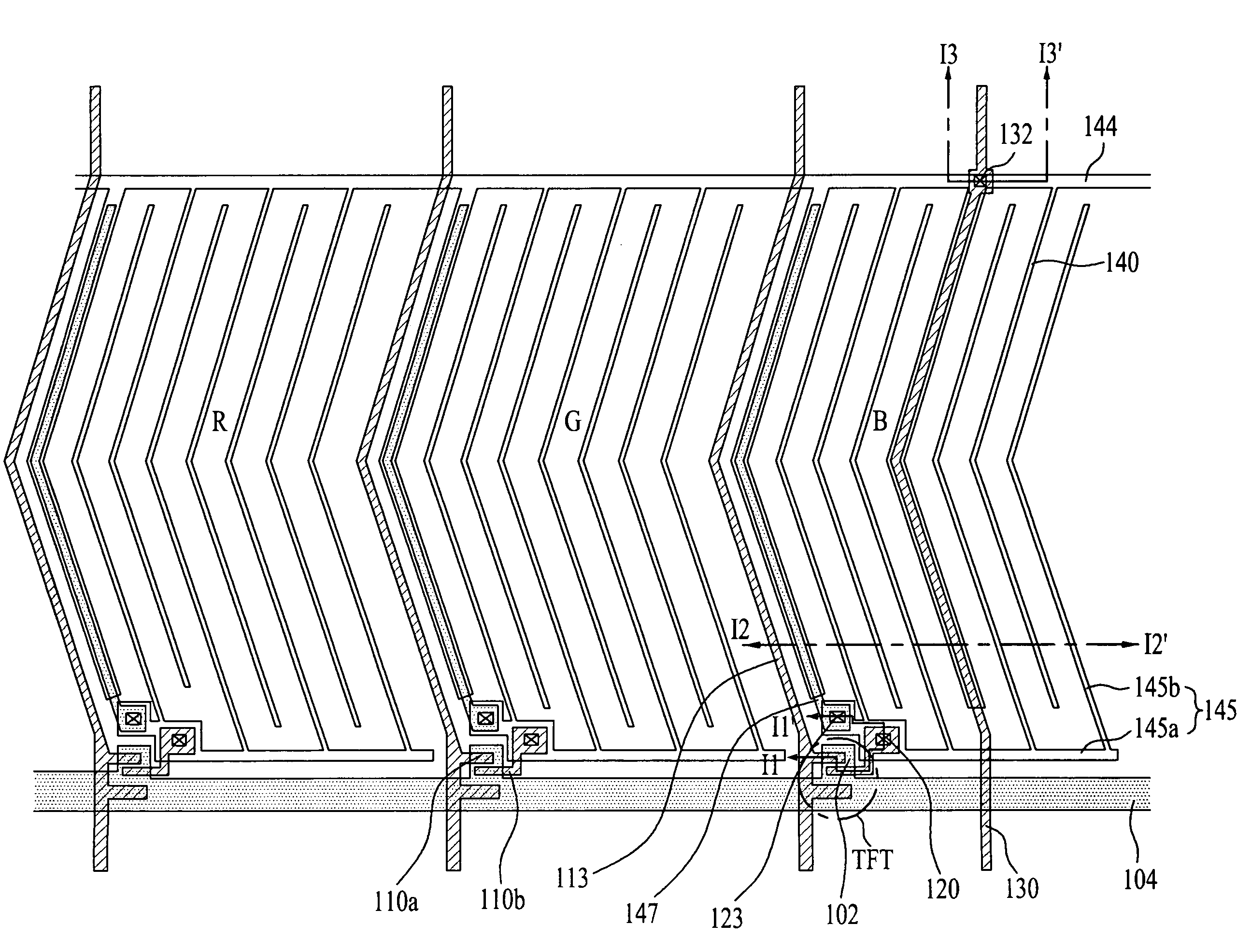
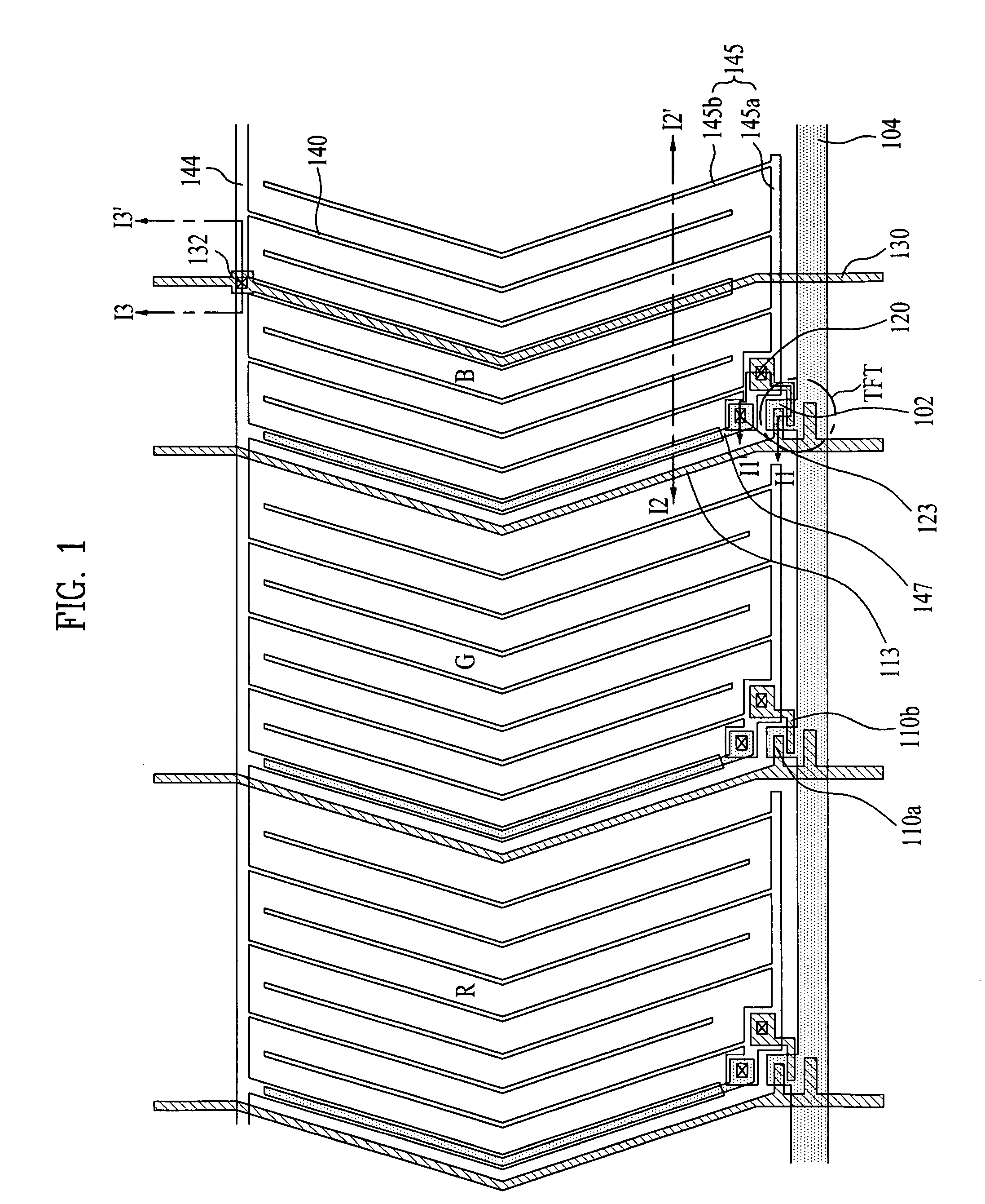
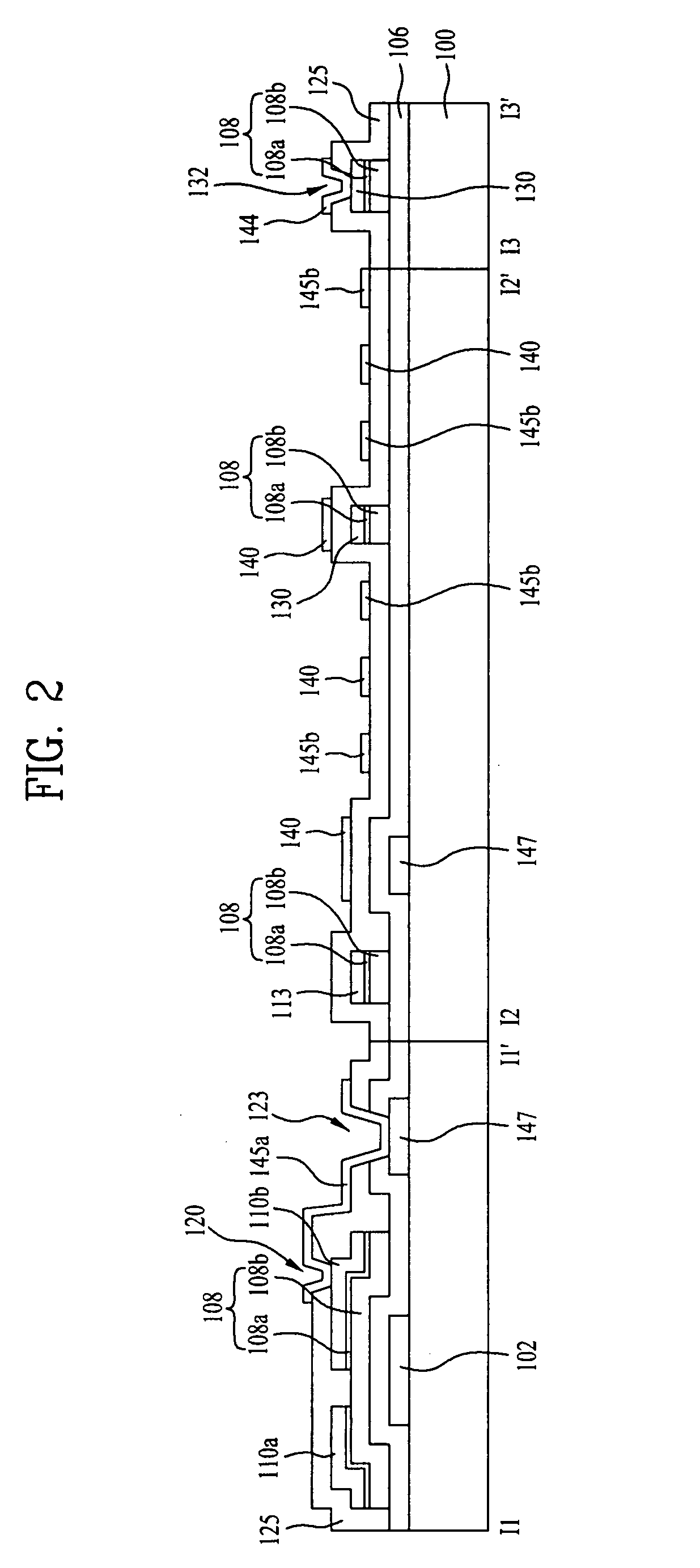
[0032]FIG. 1 is a plan view illustrating a thin film transistor substrate of an in-plane switching (IPS) liquid crystal display (LCD) device according to the present invention. FIG. 2 is a cross-sectional view taken along the lines I1-I1′ to I3-I3′ of FIG. 1, illustrating the thin film transistor substrate.
[0033]The IPS LCD device shown in FIGS. 1 and 2 includes a thin film transistor substrate 100 defined with a plurality of pixel regions each having red (R), green (G), and blue (B) sub-pixel regions. The IPS LCD device also includes a plurality of gate lines 104 formed on the substrate 100, and a plurality of data lines 113 formed on the substrate 100 to intersect with the gate lines 104 under the condition in which a gate insulating film 106 is interposed between the gate lines 104 and the data lines 113, and thus to define the sub-pixel regions. The IPS LCD device further includes thin film transistors TFT formed at respective intersections of the gate lines 104 and data lines 1...
second embodiment
[0058]FIG. 4 is a plan view illustrating a thin film transistor substrate of an IPS LCD device according to the present invention. FIG. 5 is a cross-sectional view taken along the lines II1-II1′ to II3-II3′ of FIG. 4, illustrating the thin film transistor substrate.
[0059]No description will be given of the constituent elements of the IPS LCD device shown in FIG. 4, which are identical to those of the thin film transistor substrate in the IPS LCD device shown in FIG. 1.
[0060]Referring to FIGS. 4 and 5, the data lines 113 respectively formed in the R and G sub-pixel regions of each pixel region are arranged adjacent to each other. Also, the thin film transistors TFT respectively formed in the R and G sub-pixel regions of each pixel region are arranged adjacent to each other.
[0061]Each common electrode 140 has a horizontal portion 140a formed to be parallel to the corresponding gate line 104, a finger portion 140b connected to the horizontal portion 140a, to form a horizontal electric ...
third embodiment
[0067]FIGS. 6 to 9 are views illustrating a thin film transistor substrate of an IPS LCD device according to the present invention.
[0068]No description will be given of the constituent elements of the IPS LCD device shown in FIGS. 6 to 9, which are identical to those of the first and second embodiments.
[0069]Referring to FIG. 6, the data lines 113 respectively formed in the R and G sub-pixel regions of each pixel region are arranged adjacent to each other. Also, the thin film transistors TFT respectively formed in the R and G sub-pixel regions of each pixel region are arranged adjacent to each other. The data line 113 formed in the B sub-pixel region of each pixel region is arranged at the right side of the B sub-pixel region. In each pixel region, the corresponding vertical common line includes a first vertical common line 134a formed at the left side of the R sub-pixel region, and a second vertical common line 134b formed to be shared by the G and B sub-pixel regions. The first an...
PUM
| Property | Measurement | Unit |
|---|---|---|
| width | aaaaa | aaaaa |
| width | aaaaa | aaaaa |
| width | aaaaa | aaaaa |
Abstract
Description
Claims
Application Information


