
Input device

a technology of input device and capacitance, which is applied in the field of input device, can solve the problems of increasing manufacturing costs, reducing the detection accuracy of the variation in capacitance by difficult to use the capacitance-type detecting portion, so as to reduce the thickness of the input device, reduce manufacturing costs, and reduce the number of layers

Inactive Publication Date: 2009-08-27
ALPS ALPINE CO LTD
View PDF4 Cites 40 Cited by
  • Summary
  • Abstract
  • Description
  • Claims
  • Application Information

AI Technical Summary

Benefits of technology

[0011]In the input device according to the above-mentioned aspect of the invention, no metal shield layer is provided between the pressure sensitive detecting portion and the capacitance-type detecting portion provided on the pressure sensitive detecting portion. Therefore, it is possible to decrease the number of layers of the detecting portions and reduce the thickness of an input device. In addition, it is possible to reduce manufacturing costs. Further, since no metal layer is provided, it is possible to reduce the rigidity of layers provided above the pressure sensitive detecting portion. Therefore, when the surface of the input device is pressed, it is easy to operate the pressure sensitive detecting portion.

Problems solved by technology

In the input device, when a voltage is applied to a conductive layer or a resistor layer of the pressure sensitive detecting portion, the detection accuracy of the variation in capacitance by the capacitance-type detecting portion is significantly lowered due to charge in the layer, and it is difficult to use the capacitance-type detecting portion.
As a result, manufacturing costs increase, and it is difficult to reduce the thickness of an input device.
Therefore, when the surface of the input device is pressed by, for example, an input pen, the entire input device is not easily deformed, and the detection accuracy of the pressure sensitive detecting portion is lowered.

Method used


Image

  • Input device
  • Input device
  • Input device

Examples


Embodiment Construction

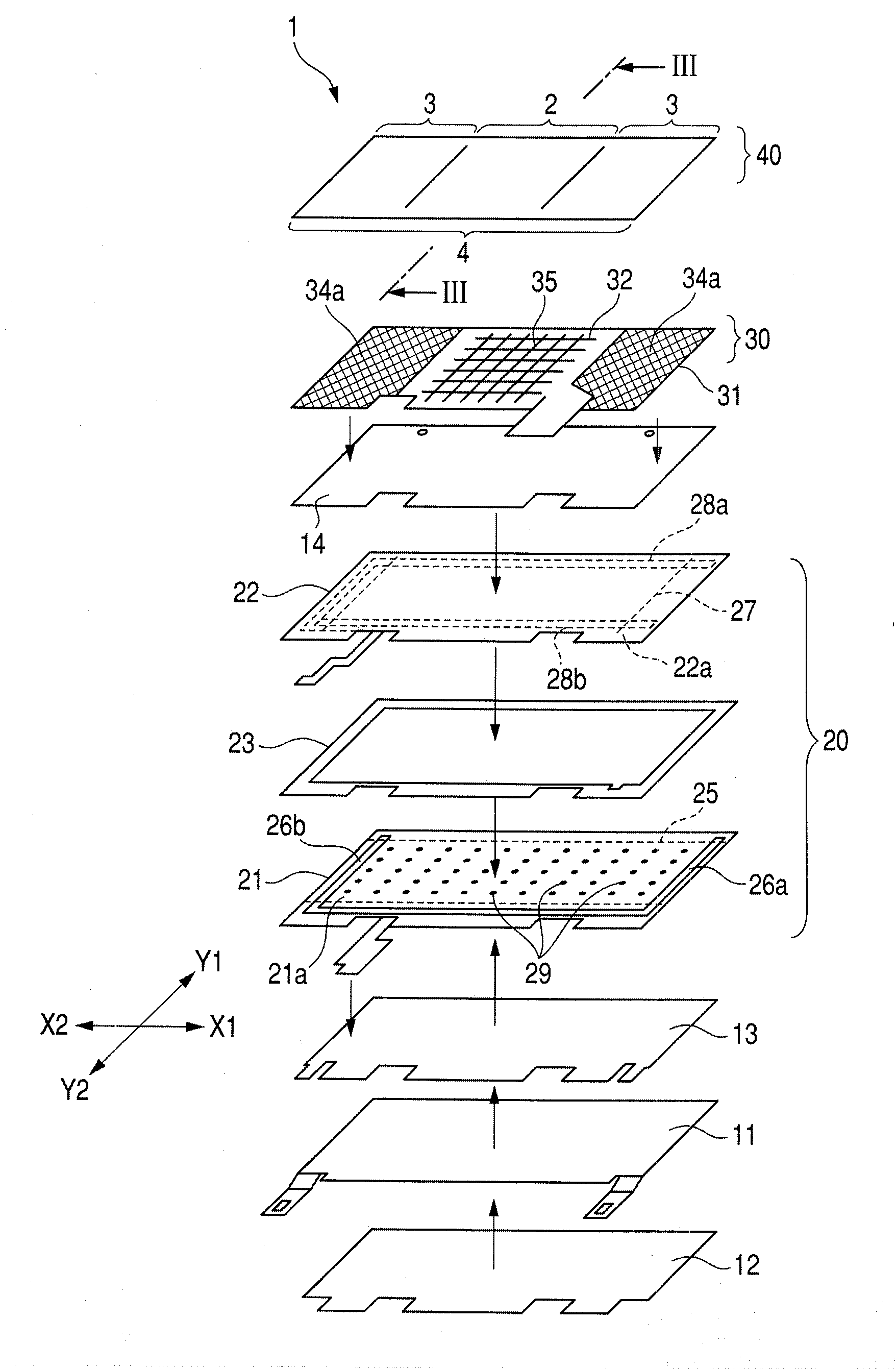
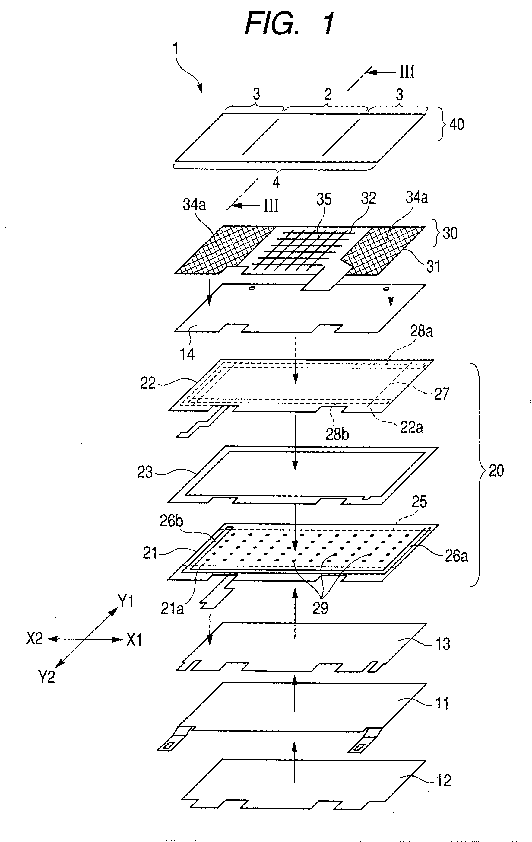
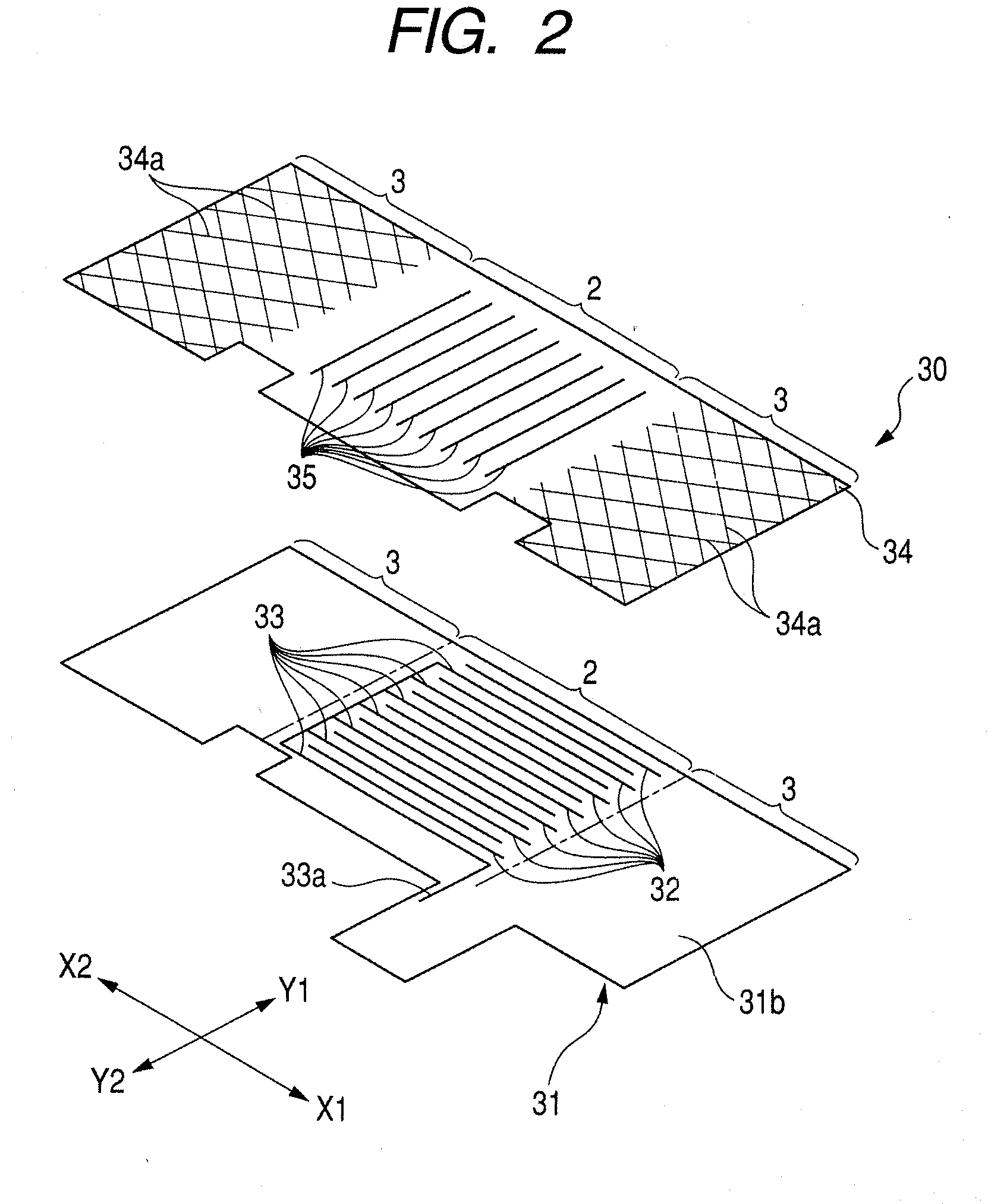
[0017]FIG. 1 is an exploded perspective view illustrating an input device according to a first embodiment of the invention. FIG. 2 is an exploded perspective view illustrating the structure of a pressure sensitive detecting portion of the input device. FIG. 3 is a partial enlarged cross-sectional view illustrating the input device according to the first embodiment taken along the line III-III of FIG. 1.

[0018]As shown in FIGS. 1 and 2, an input device 1 according to the first embodiment has a rectangular shape having a long side aligned with the X direction and a short side aligned with the Y direction. The center of the input device 1 in the X direction is an electrostatic detection region 2, and both sides of the center are extending portions 3. Substantially the entire region including the electrostatic detection region 2 and the extending portions 3 is a pressure detection region 4. FIG. 3 is a traverse cross-sectional view of an electrostatic detection region 2.

[0019]A laminated...


PUM


Abstract

Disclosed is an input device capable of decreasing the number of layers of a detecting portion to reduce manufacturing costs and easily deforming layers provided above a pressure sensitive detecting portion. A capacitance-type detecting portion that detects the contact position of a finger on the basis of a variation in capacitance is provided on a pressure sensitive detecting portion that includes a lower detection layer formed on a lower base sheet and an upper detection layer formed on an upper base sheet. A voltage is applied to the pressure sensitive detecting portion and the capacitance-type detecting portion such that the application times of the voltages do not overlap each other. Therefore, it is possible to prevent interference between the detection operations of the two detecting portions.

Description

CLAIM OF PRIORITY[0001]This application claims benefit of the Japanese Patent Application No. 2008-40092 filed on Feb. 21, 2008, the entire content of which is hereby incorporated by reference.BACKGROUND[0002]1. Technical Field[0003]The present disclosure relates to an input device in which a pressure sensitive detecting portion that detects a pressed position on the basis of a variation in resistance value overlaps a capacitance-type detecting portion that detects the approach position of an indicator, such as a finger, on the basis of a variation in capacitance, and which is formed of a soft material, has a small thickness, and can maintain the detection accuracy of the detecting portions at a high level.[0004]2. Related Art[0005]JP-A-2001-243010 discloses an input device provided in, for example, a personal computer. In the disclosed input device, a capacitance-type detecting portion that detects the approach of a conductive indicator, such as a finger, on the basis of a variatio...

Claims


Application Information

Patent Timeline
IPC IPC(8): G06F3/041
CPCG06F3/0414G06F3/045G06F3/044G06F3/0416G06F3/0446G06F3/0445G06F3/04166
Inventor KONDO, TAKASHISHIGA, SADAKAZUKISHINO, SHINGO
Owner ALPS ALPINE CO LTD
Learn More