
Led device having improved color

a technology of led devices and color, which is applied in the manufacture of electrode systems, electric discharge tubes/lamps, and discharge tubes luminescnet screens, etc., can solve the problems of reducing device efficiency, difficult to scale to large substrates, and patterned organic material deposition technology, so as to increase the light output and manufacturability of led devices, and reduce any angular color change

Active Publication Date: 2009-08-27
GLOBAL OLED TECH
View PDF9 Cites 30 Cited by
  • Summary
  • Abstract
  • Description
  • Claims
  • Application Information

AI Technical Summary

Benefits of technology

[0013]The present invention has the advantage that it increases the light output and manufacturability of an LED device, and reduces any angular color change.

Problems solved by technology

Because LED devices employ high-optical-index emissive materials, a large fraction (e.g. greater than 50%) of the emitted light is trapped in the device due to total internal reflection and thus reduces the device efficiency.
While such designs are useful, they require a patterned organic material deposition technology (for example, vacuum deposition through metal shadow-masks) that is difficult to scale to large substrates.
Moreover, optical cavity devices typically suffer from an unacceptable angular color dependence.
However, while useful, such an approach does not improve the manufacturability of the device and provides inadequate ambient contrast ratio under some illumination conditions.
Moreover, the color filters absorb light emitted from the light-emitting layer, thereby reducing device efficiency.
Such designs, however, may have increased manufacturing costs, lower light output than desired, and reflectance larger than may be desired, as well as significant color change at different viewing angles, owing to the change in the effective optical path length for light traveling at angles to the normal.
Again such designs may have increased manufacturing costs due to patterned deposition processes.
Also, significant light may be absorbed by the color filters thereby reducing efficiency.
However, the use of color filters substantially reduces the efficiency of the device.
However, this disclosure does not address angular color issues or the large amount of trapped light.
However, this design employs a patterned semi-transparent electrode to form the white subpixel that can be difficult to manufacture in a top-emitting format.
However, applicants have demonstrated that, within an LED area-emissive display, the formation of adjacent film structures having significantly different thicknesses or sharp edges on a substrate, can cause electrical shorts in the device when films are not deposited over the edges.

Method used


Image

  • Led device having improved color
  • Led device having improved color
  • Led device having improved color

Examples


Embodiment Construction

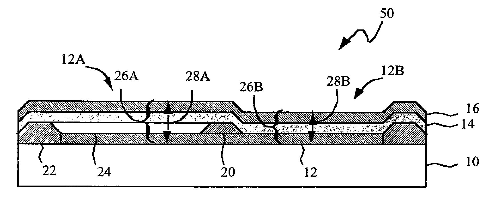
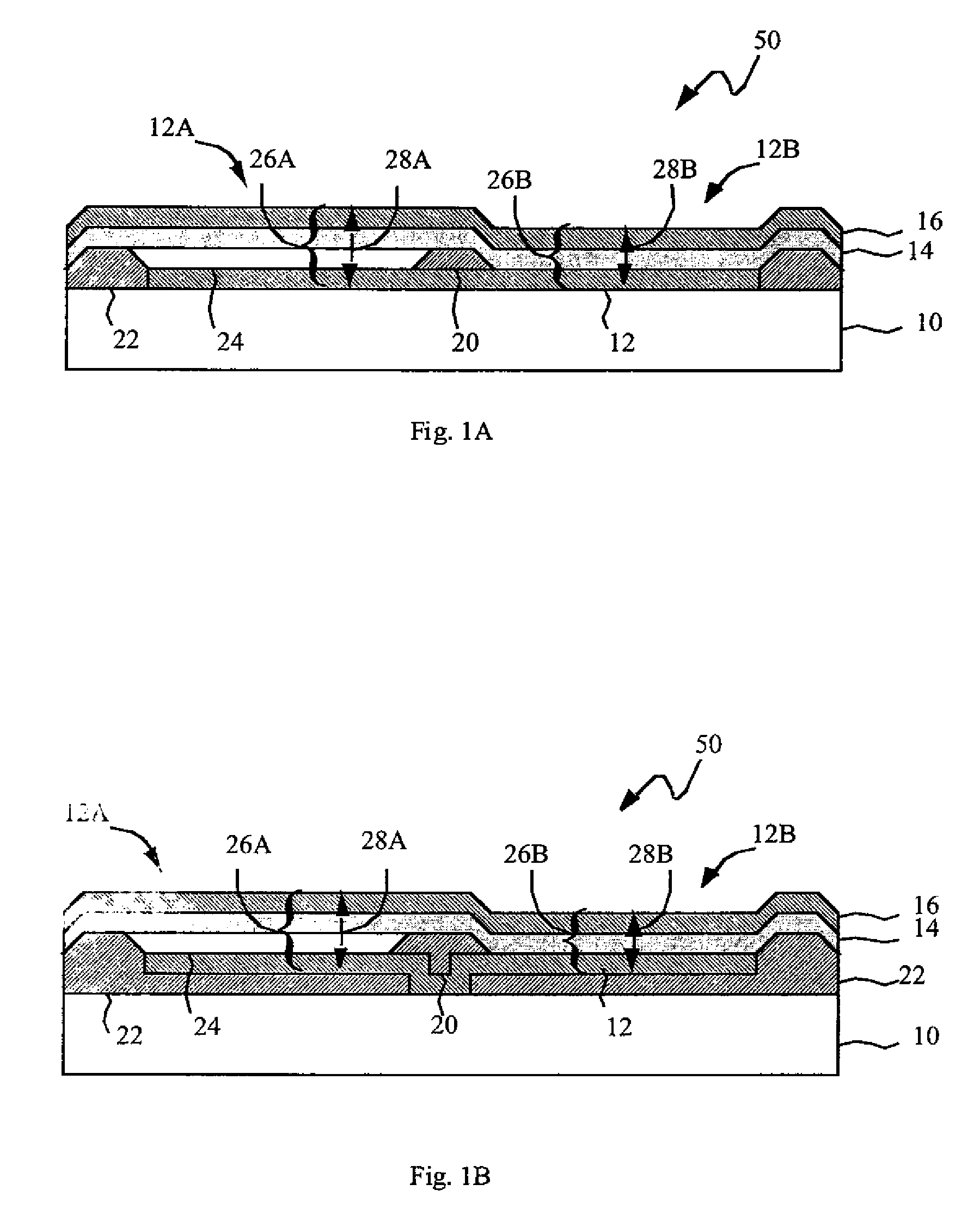
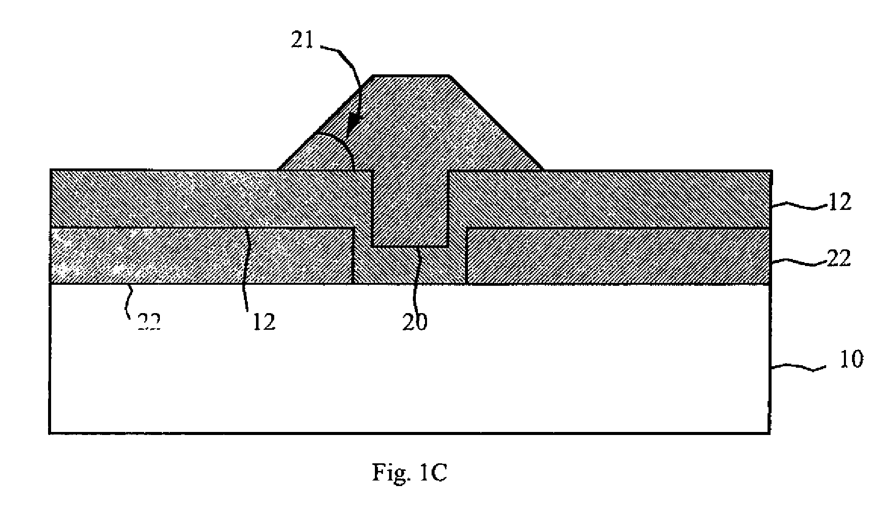
[0025]Referring to FIGS. 1A and 1B, a display device according to an embodiment of the present invention comprises a substrate 10 having at least one light-emitting element 50, the light-emitting element 50 including one electrically-continuous electrode 12 formed over the substrate 10, a separator 20 located on the electrically-continuous electrode 12 dividing the surface of the electrically-continuous electrode 12 into first and second electrode portions 12A, 12B, the electrode portions 12A, 12B electrically continuous with each other, a transparent layer 24 located over the first electrode portion (e.g. 12A), the transparent layer 24 separated by the separator 20 from the second electrode portions, a light-emitting layer 14 formed over the transparent layer 24 and the electrode portion 12B, a second electrode 16 formed over the light-emitting layer 14, and wherein the first electrode portion 12A, the transparent layer 24, the light-emitting layer 14, and the second electrode 16 c...


PUM


Abstract

A display device includes a substrate having at least one light-emitting element. The light-emitting element includes one electrically-continuous electrode formed over the substrate. A separator is located on the electrically-continuous electrode, dividing the electrically-continuous electrode into at least first and second separate electrode portions that remain electrically continuous. A transparent layer is located over the first electrode portion, while separated from the second electrode portion. A light-emitting layer is formed over the transparent layer and the second electrode portion. A second electrode is formed over the light-emitting layer. The first electrode portion, the transparent layer, the light-emitting layer, and the second electrode comprise a first optical cavity having a first optical path length. The second electrode portion, the light-emitting layer, and the second electrode comprise a second optical cavity having a second optical path length different from the first optical path length.

Description

FIELD OF THE INVENTION[0001]The present invention relates to light-emitting diode (LED) devices, and more particularly, to organic and inorganic LED device structures for improving light output, color, manufacturability, and angular performance.BACKGROUND OF THE INVENTION[0002]Emissive flat-panel display devices are widely used in conjunction with computing devices and in particular with portable devices. These displays are often used in public areas with significant ambient illumination and are viewed from a wide variety of angles. Such devices are also under development as area illumination devices or lamps.[0003]Light-emitting diodes (LED) incorporating thin films of light-emitting materials have many advantages in a flat-panel display device and are useful in optical systems. Such films can comprise either, or both, organic and inorganic materials. U.S. Pat. No. 6,384,529 issued May 7, 2002 to Tang et al. shows an OLED color display that includes an array of OLED light emitting ...

Claims


Application Information

Patent Timeline
Patent Type & Authority Applications(United States)
IPC IPC(8): H01J1/62H01L27/28H01J9/02
CPCH01L27/3213H01L27/3244H01L27/3246H01L51/5265H01L27/3283H01L51/5036H01L27/3281H10K59/351H10K59/122H10K59/12H10K59/173H10K50/125H10K59/876H10K50/852H10K59/17
Inventor COK, RONALD S.
Owner GLOBAL OLED TECH
Features
  • Generate Ideas
  • Intellectual Property
  • Life Sciences
  • Materials
  • Tech Scout
  • Unparalleled Data Quality
  • Higher Quality Content
  • 60% Fewer Hallucinations
Learn More