

Electro-optical device and electronic apparatus
- Summary
- Abstract
- Description
- Claims
- Application Information
AI Technical Summary
Benefits of technology
Problems solved by technology
Method used
Image

Examples
first embodiment
Electro-Optical Device
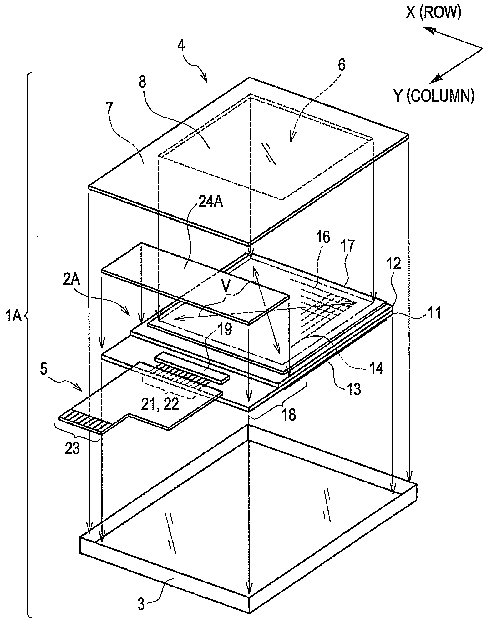
[0123]Hereinafter, an embodiment of the invention will be described with reference to the drawings. Although the following description will be provided with reference to the drawings, in terms of ease of understanding of distinctive portions, the constituent elements in the drawings may be shown on a scale different from that of the actual constituent elements.
[0124]FIG. 1 shows a liquid crystal display which is an example of an electro-optical device according to this embodiment. A liquid crystal display 1A includes a liquid crystal panel 2A serving as a panel, an FPC (Flexible Printed Circuit) board 5, serving as a wiring board, connected to the liquid crystal panel 2A, a lower frame 3, and a protective cover 4 serving as a protective member or a receiving member. When the liquid crystal panel 2A is a transmissive liquid crystal panel, a backlight, serving as an illumination device, which is not shown in FIG. 1, is provided between the lower frame 3 and the l...
second embodiment
Electro-Optical Device
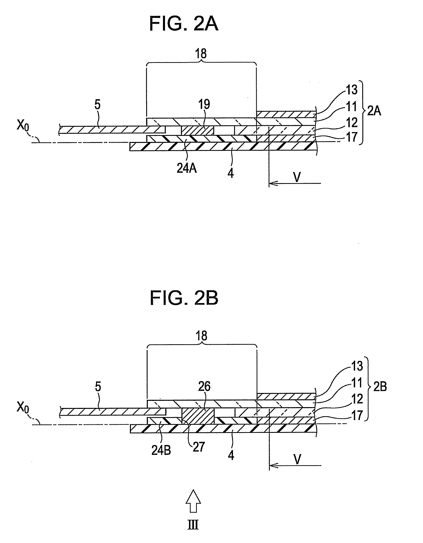
[0149]FIGS. 2B and 3 show a liquid crystal panel 2B that is a main part of a liquid crystal display serving as an electro-optical device of this embodiment. FIG. 2B shows a side sectional structure of main parts of the liquid crystal panel 2B, and FIG. 3 shows a planar structure when viewed from an arrow III of FIG. 2B. In FIG. 3, the protective cover 4 is not shown. Instead of the liquid crystal panel 2A of FIG. 1, the liquid crystal panel 2B shown in FIGS. 2B and 3 is housed in the lower frame 3, and is received and protected by the protective cover 4.
[0150]In FIG. 2B, the liquid crystal panel 2B has the same configuration as the liquid crystal panel 2A of the first embodiment shown in FIG. 2A, excluding a driving IC 26. The same parts are represented by the same reference numerals, and descriptions thereof will be omitted. The height of the driving IC 19 used in the liquid crystal panel 2A of FIG. 2A is substantially equal to the thickness of the color filte...
third embodiment
Electro-Optical Device
[0154]FIG. 4A shows a liquid crystal panel 2C that is a main part of a liquid crystal display serving as an electro-optical device of this embodiment. Instead of the liquid crystal panel 2A of FIG. 1, the liquid crystal panel 2C is housed in the lower frame 3 and is protected by the protective cover 4 serving as a protective member. The liquid crystal panel 2C has an element substrate 31, a polarizing plate 33 adhered to the outer surface of the element substrate 31, a color filter substrate 32, and a polarizing plate 37, serving as a surface member, adhered to the outer surface of the color filter substrate 32.
[0155]Like the element substrate 11 shown in FIG. 1, on the element substrate 31, a plurality of source lines 14 are formed so as to extend in the column direction Y, and a plurality of gate lines 16 are formed so as to extend in the row direction X perpendicular to the column direction Y. In each rectangular planar region surrounded by the source lines ...
PUM
 Abstract
Description
Claims
Application Information