Semiconductor device with solder balls having high reliability

Active Publication Date: 2007-05-03
RENESAS ELECTRONICS CORP
View PDF11 Cites 3 Cited by
  • Summary
  • Abstract
  • Description
  • Claims
  • Application Information

AI Technical Summary

Benefits of technology

[0015] According to the present invention, since the alloy layer includes Ni and Zn, the impact resistance is high, and the reliability of the connection between the metal layer and solder ball is superior. Moreover, since the Sn—Ag—Cu-based solder ball i

Problems solved by technology

Thus, there was a case that the connection reliability was reduced.
However, since the Sn—Zn-based solder was low

Method used


Image

  • Semiconductor device with solder balls having high reliability
  • Semiconductor device with solder balls having high reliability
  • Semiconductor device with solder balls having high reliability

Examples


first embodiment

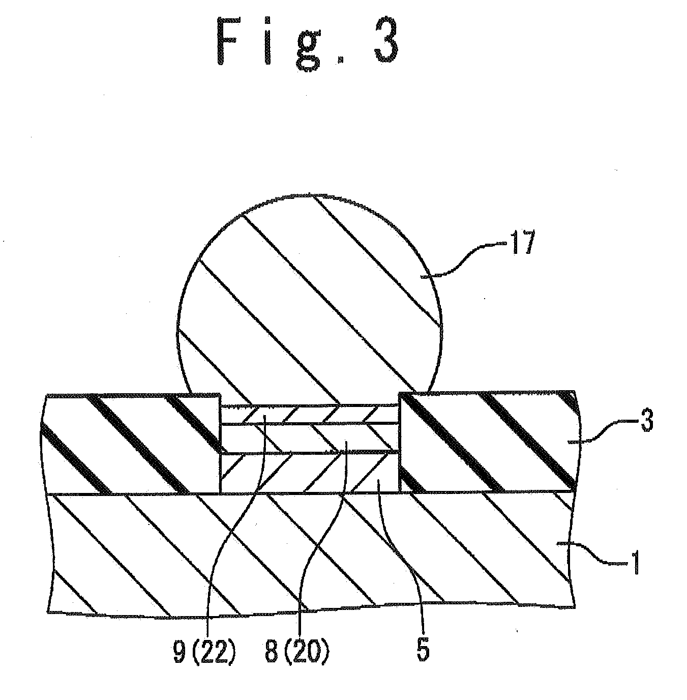
[0030] As shown in FIG. 3, in the semiconductor device of the first embodiment, a solder resist 3 having an opening is formed on the substrate 1. A Cu layer 5, a Ni layer 8 and an alloy layer are laminated in turn inside this opening.

[0031] In this embodiment, the alloy layer is the Ni—Zn alloy layer 9 composed of Ni and Zn. The Sn—Ag—Cu-based solder ball 17 is installed on the surface of the Ni—Zn alloy layer 9.

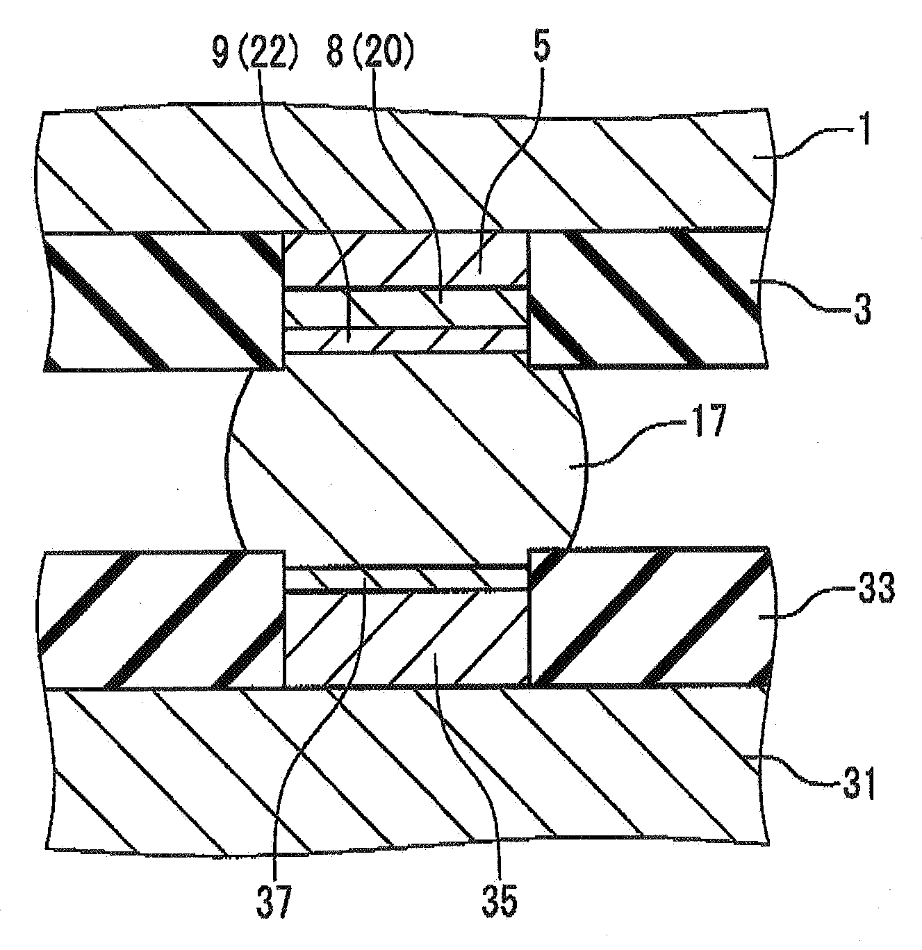
[0032]FIG. 4 is a sectional view showing an example that the semiconductor device of the first embodiment is installed on a mount substrate.

[0033] As shown in FIG. 4, a solder resist 33 having an opening is formed on a substrate 31, in the mount substrate. A Cu layer 35 and an alloy layer (hereafter, referred to as a Cu—Sn alloy layer 37) composed of Cu and Zn are laminated inside this opening. The Sn—Ag—Cu-based solder ball 17 is adhered through the Cu—Sn alloy layer 37 to the Cu layer 35, In this way, the Cu—Sn alloy layer 37 is formed between the mount substrate and th...

second embodiment

[0046] A semiconductor device in the second embodiment differs from the semiconductor device in the first embodiment in that an alloy layer is an alloy layer (Ni—Au—Zn alloy layer 22) composed of Ni, Au and Zn.

[0047] A method of manufacturing the semiconductor device of the second embodiment as mentioned above will be described below with reference to drawings. FIGS. 9 to 13 are sectional views showing the method of manufacturing the semiconductor device of the second embodiment.

[0048] The method of manufacturing the semiconductor device of the second embodiment includes the following steps of:

(1) forming the solder resist 3 having the opening on the substrate 1 (FIG. 9);

(2) forming a Ni inclusion plating layer (the Cu layer 105, a Ni layer 18 and an Au layer 19) inside the opening (FIG. 9), and

(3) installing the Sn—Ag—Cu-based solder ball 17 through the alloy layer (the Ni—Au—Zn alloy layer 22), which includes Ni and Zn as the essential components, on the Ni inclusion plati...

third embodiment

[0056] A semiconductor device in the third embodiment differs from the semiconductor device in the first embodiment in that the alloy layer is the Ni—Au—Zn alloy layer 22.

[0057] A method of manufacturing the semiconductor device of the third embodiment as mentioned above will be described below with reference to drawings. FIGS. 14 to 16 are sectional views showing the method of manufacturing the semiconductor device of the third embodiment.

[0058] The method of manufacturing the semiconductor device of the third embodiment includes the following steps of:

(1) forming the solder resist 3 having the opening on the substrate 1 (FIG. 14);

(2) forming the Ni inclusion plating layer (the Cu layer 5, the Ni layer 18 and the Au layer 19) inside the opening (FIG. 14); and

(3) installing a Sn—Ag—Cu-based solder ball 25 through the alloy layer (the Ni—Au—Zn alloy layer 22), which includes Ni and Zn as the essential components, on the Ni inclusion plating layer (FIGS. 15 and 16).

[0059] The...


PUM


Abstract

A semiconductor device includes a substrate, a metal layer, an alloy layer and a Sn—Ag—Cu-based solder ball. The metal layer is configured to be formed on the substrate. The alloy layer is configured to be formed on the metal layer. The Sn—Ag—Cu-based solder ball is configured to be placed on the alloy layer. The alloy layer includes Ni and Zn as essential elements.

Description

BACKGROUND OF THE INVENTION [0001] 1. Field of the Invention [0002] The present invention relates to a semiconductor device. More particularly, the present invention relates to a semiconductor device with solder balls as external connection terminals having high reliability. [0003] 2. Description of the Related Art [0004] Conventionally, Sn—Pb eutectic solder has been used. However, since a lead-free solder is requested, various solders are developed. [0005] For example, Japanese Laid-Open Patent Application JP-A-Heisei, 5-50286 discloses one of such solders. The solder (hereafter, referred to as Sn—Ag—Cu-based Solder) is composed of: Ag between 3.0 and 5.0 weight %; Cu between 0.5 and 3.0 weight %; and Sn of the remainder. The solder ball of such composition is actually used as the external connection terminal of BGA (Ball Grid Array). [0006]FIG. 1 is a sectional view showing a conventional semiconductor device. As shown in FIG. 1, in the conventional semiconductor device, a solder...

Claims


Application Information

Patent Timeline
IPC IPC(8): H01L23/48
CPCH01L24/02H01L2224/0401H01L2224/11334H01L24/13H01L24/11H01L2224/13099H01L2924/01004H01L2924/01005H01L2924/01028H01L2924/01029H01L2924/0103H01L2924/01046H01L2924/01047H01L2924/0105H01L2924/01061H01L2924/01078H01L2924/01079H01L2924/01082H01L2924/01322H01L2924/01327H01L2924/014H05K3/244H05K3/3463H01L2924/01006H01L2924/01033H01L2224/11849H01L2224/119H01L2924/00H01L2224/11H01L2224/13H01L24/03H01L24/05
Inventor KAWASHIRO, FUMIYOSHI
Owner RENESAS ELECTRONICS CORP
Why Eureka
Try Eureka