Semiconductor device and method of producing the same

Active Publication Date: 2009-09-10
FUJI ELECTRIC CO LTD
View PDF5 Cites 92 Cited by
  • Summary
  • Abstract
  • Description
  • Claims
  • Application Information

AI Technical Summary

Benefits of technology

[0014]The present invention relates to a semiconductor device, such as a diode or an IGBT, having soft recov

Problems solved by technology

Consequently, so-called snappy reverse recovery (hard recovery) occurs so that both reverse recovery voltage and current can produce undesirable oscillated waveforms.
Specifically, there is a problem awaiting solution that implantation of a low concentration of minority carriers into

Method used


Image

  • Semiconductor device and method of producing the same
  • Semiconductor device and method of producing the same
  • Semiconductor device and method of producing the same

Examples


first embodiment

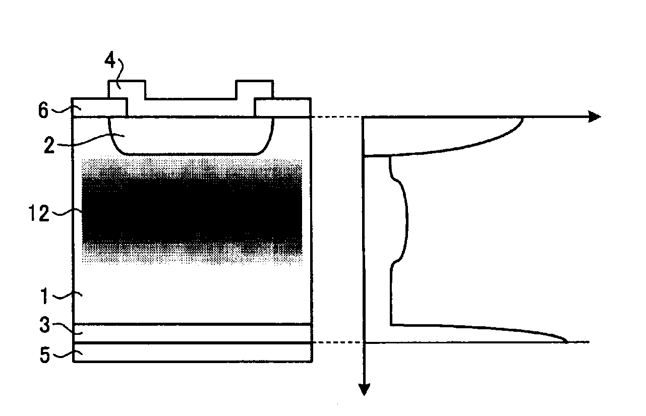
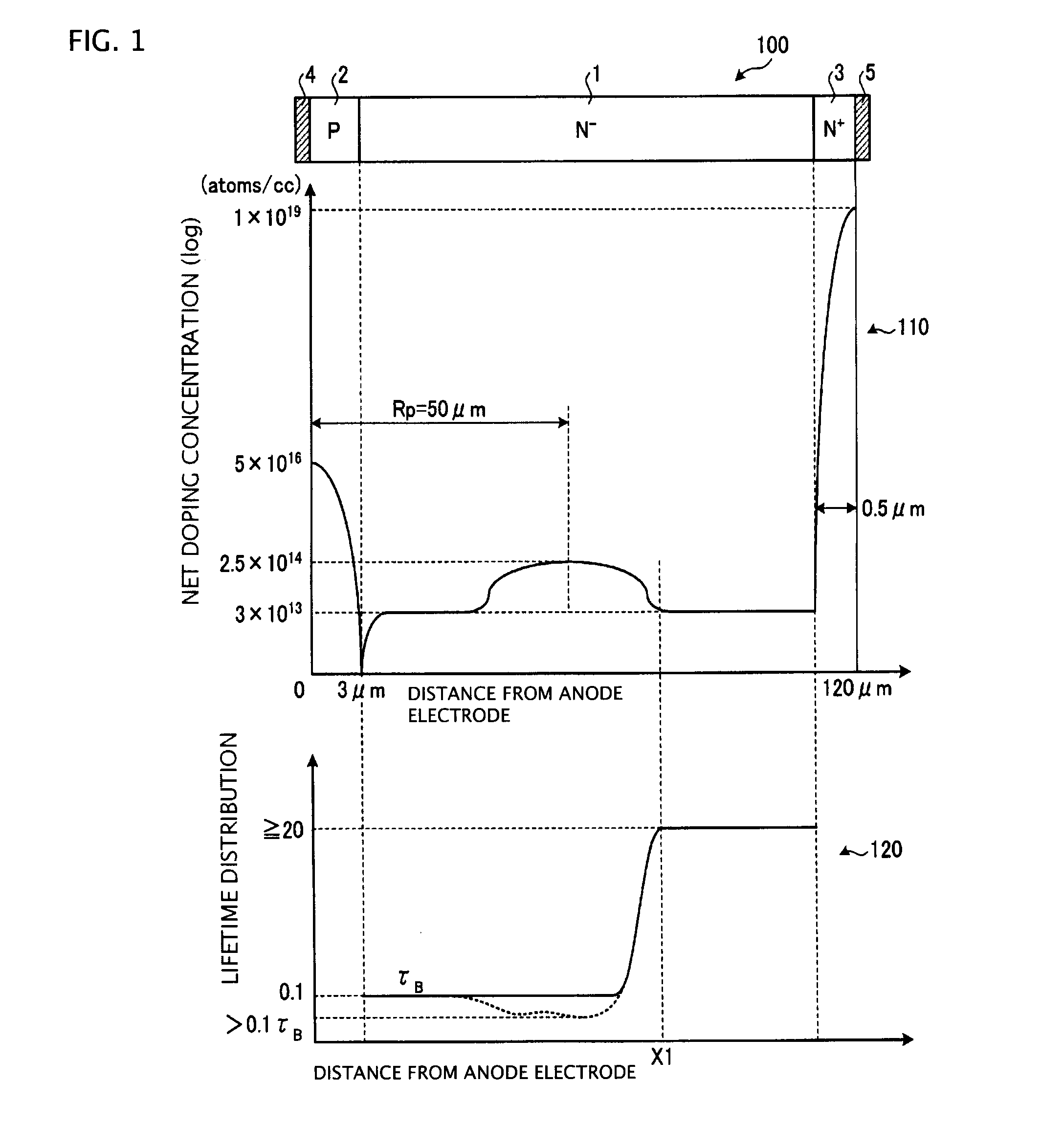
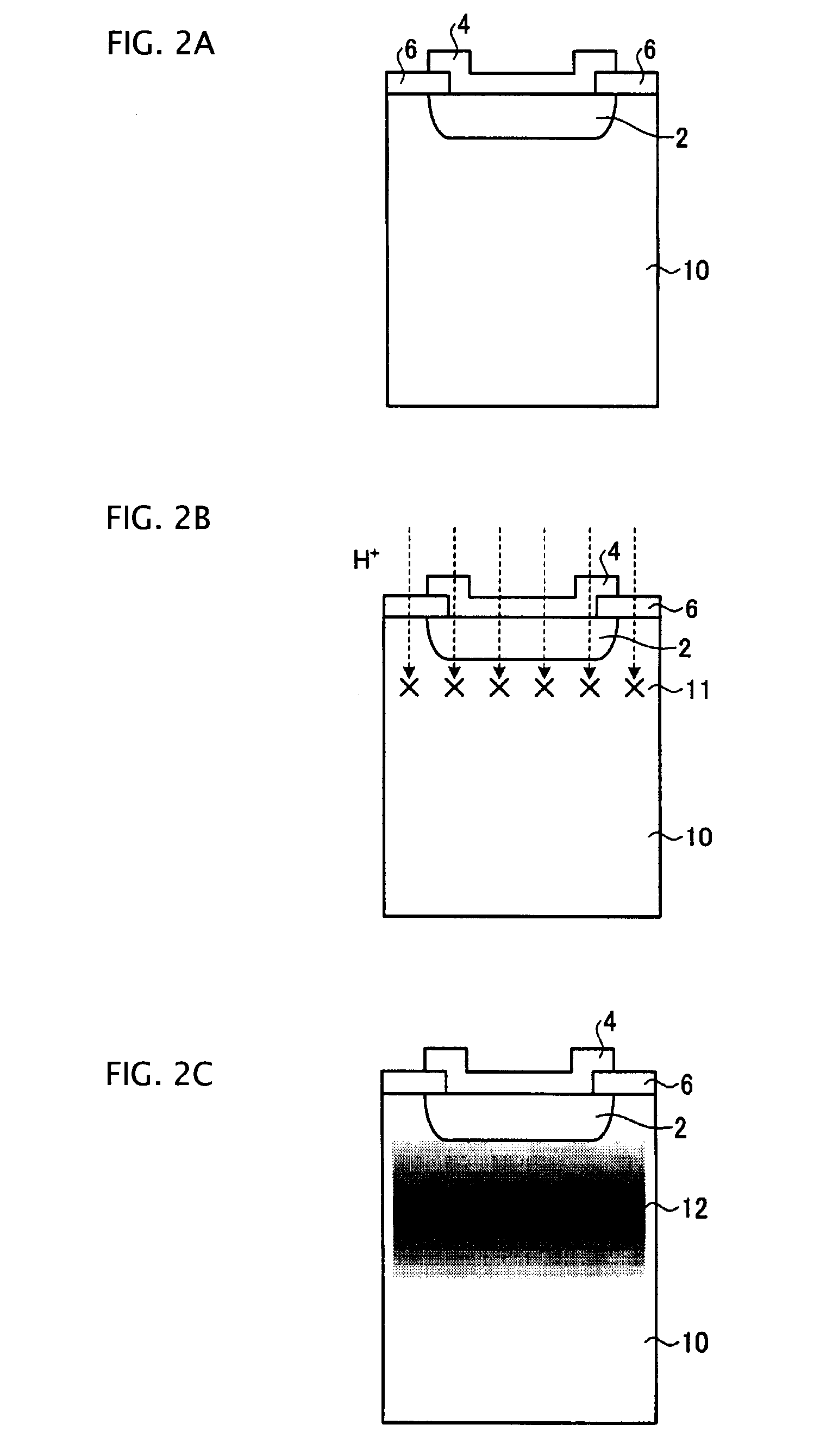
[0053]Referring to FIG. 1, a semiconductor device 100 (first embodiment) has a second semiconductor layer 2 of a P type serving as a P anode layer formed on one principal surface of a first semiconductor layer 1 (i.e., semiconductor substrate) of an N type serving as an N− drift layer. A third semiconductor layer 3 of the N type serving as an N+ cathode layer is formed on the other principal surface of the first semiconductor layer 1. An anode electrode 4 is formed on a surface of the second semiconductor layer 2. A cathode electrode 5 is formed on a surface of the third semiconductor layer 3.

[0054]As shown in a characteristic graph 110 of distance from the anode electrode versus net doping concentration (log) in FIG. 1, the net doping concentration of the first semiconductor layer 1 has a peak near its midpoint and decreases with a gradient toward the second and third semiconductor layers 2 and 3. That is, in the first embodiment, the semiconductor device 100 has a broad buffer str...

second embodiment

[0131]Referring to FIG. 20, which illustrates the second embodiment, the semiconductor device 200 includes a fourth semiconductor layer 31 as an N+ cathode stopper layer disposed between the third semiconductor layer 3 as an N++ cathode layer and the first semiconductor layer 1 as an N− drift layer, and higher in concentration than the bulk concentration and lower in concentration than the third semiconductor layer 3.

[0132]The fourth semiconductor layer 31 is a high concentration stopper layer for stopping a depletion layer at a depth of 5-20 μm. Various defects, such as roughness and particles produced in grinding, are produced in the rear surface of the wafer. The fourth semiconductor layer 31 can prevent the depletion layer spread at the time of reverse biasing from reaching the defects in the rear surface of the wafer and accordingly, can prevent the leakage current from increasing. The provision of the fourth semiconductor layer 31 permits the percentage of leakage current defe...


PUM


Abstract

A semiconductor substrate and a method of its manufacture has a semiconductor substrate having a carbon concentration in a range of 6.0×10¹⁵ to 2.0×10¹⁷ atoms/cm3, both inclusively. One principal surface of the substrate is irradiated with protons and then heat-treated to thereby form a broad buffer structure, namely a region in a first semiconductor layer where a net impurity doping concentration is locally maximized. Due to the broad buffer structure, lifetime values are substantially equalized in a region extending from an interface between the first semiconductor layer and a second semiconductor layer formed on the first semiconductor layer to the region where the net impurity doping concentration is locally maximized. In addition, the local minimum of lifetime values of the first semiconductor layer becomes high. It is thus possible to provide a semiconductor device having soft recovery characteristics, in addition to high-speed and low-loss characteristics, while suppressing a kinked leakage current waveform.

Description

BACKGROUND[0001]There are diodes, Insulated Gate Bipolar Transistors (IGBTs), etc., of a 600V, 1200V, or 1700V withstand voltage class, as power semiconductor devices. Improvements of characteristics of these devices have advanced recently. The power semiconductor devices are used in power conversion systems, such as a high-efficiency power-saving converter-inverter system, and essential for controlling rotation motors and servomotors.[0002]Characteristics of low loss, power saving, high speed, high efficiency, and environmental friendliness, i.e., no bad influence on surroundings are required of such a power controller. For these requirements, there is commonly known a method of thinning the rear surface of a typical semiconductor substrate (e.g. silicon wafer) by grinding or the like after forming the front surface side region of the semiconductor substrate, and then performing ion implantation of an element with a predetermined concentration from the ground surface side, followed...

Claims


Application Information

Patent Timeline
IPC IPC(8): H01L29/66H01L21/26H01L21/329
CPCH01L21/2255H01L21/263H01L29/8611H01L29/66128H01L29/167
Inventor NEMOTO, MICHIO
Owner FUJI ELECTRIC CO LTD
Why Eureka
Try Eureka