Semiconductor device and manufacturing method for the same

a technology of semiconductor devices and semiconductors, applied in semiconductor devices, diodes, electrical apparatus, etc., can solve problems such as element damage, and failure to meet the requirements of the circuit, and achieve the effect of high speed and soft recovery characteristics

Inactive Publication Date: 2002-10-31
FUJI ELECTRIC CO LTD
View PDF0 Cites 14 Cited by
  • Summary
  • Abstract
  • Description
  • Claims
  • Application Information

AI Technical Summary

Benefits of technology

0015] It is another object of the present invention to provide a semiconductor device and a manufacturing method for the same which provides a diode with high speed as well as soft recovery characteristics.

Problems solved by technology

When the reverse recovery current is large, this leads to an undesirable increase in the turn on loss for a MOS transistor frequently used as a switching element on the power factor improvement circuit (PFC) and also leads to an undesirable rise in temperature of the element.
If the attrition rate is large, a large voltage noise is generated and added onto the power voltage, and by having this voltage applied to the diode and MOS transistor, the element can be destroyed and errors in the circuit may result.
However, there is a `tradeoff` between the forward voltage of the diode and the reverse recovery current, and the forward voltage of the diode increases.
As a result, an adequate soft recovery is not achieved.
Therefore, the beneficial effect of the platinum is not adequate near pnjunctions that are deeper than several micrometers.
As a result, the improvement in the `tradeoff` is inadequate, and there is little if any improvement in the soft recovery characteristics.
Unfortunately, if the injection amount is increased, not only does the -type semiconductor layer become high resistance, but defects are increased due to the high platinum concentration in the P-type active region, resulting in at least an increase in leakage current.

Method used


Image

  • Semiconductor device and manufacturing method for the same
  • Semiconductor device and manufacturing method for the same
  • Semiconductor device and manufacturing method for the same

Examples


first embodiment

[0085] Referring now to FIG. 12, the results of a forward voltage VF and a reverse recovery current peak value IRP are shown. In the related art, the `trade off` resulting from Pt diffusion condition adjustments are all hard recovery. In order to have softening, the VF is increased, or in other words, this `trade off` results in a shift to the right in the graph. Therefore, compared to the tradeoffresulting from the Pt diffusion condition adjustments in the related art, the results of the present invention show that a substantial improvement in `tradeoff` is achieved.

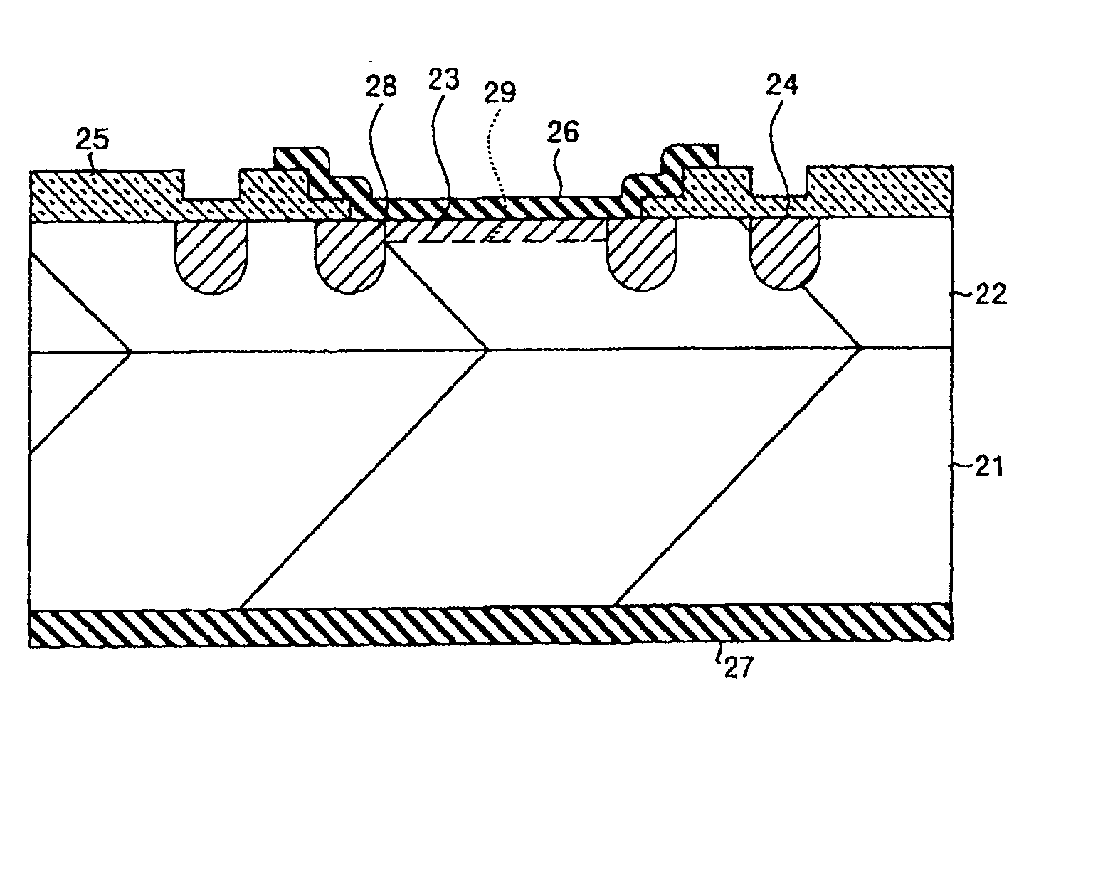
[0086] According to the present invention, by heat diffusion of platinum in -type semiconductor device 22, the region near the surface of semiconductor layer 22 reverses to a P-type. Since a shallow pn junction is formed by P-type reverse region 23 and -type semiconductor layer 22, the platinum concentration does not need to be any higher than necessary, and the pn junction is formed at a position where the effects of p...

second embodiment

[0091] Referring now to FIG. 14, the structure of a second embodiment of a semiconductor device is shown. The semiconductor device has an -type semiconductor substrate 41 doped with As (arsenic), an -type semiconductor layer 42 doped with P (phosphorus). Also included are a P-type reverse region 43, a Ptype guard ring region 44, an oxide film 45, a front electrode 46 and a back electrode 47.

[0092] As an example, the thickness of semiconductor substrate 41 is 500 micrometers, and its impurity concentration is 2.times.10.sup.19 cm.sup.-3. Also as an example, the thickness of semiconductor layer 42 is 60 micrometers, and its impurity concentration is 2.times.10.sup.14 cm.sup.-3.

[0093] A portion of the surface of semiconductor layer 42 is covered by oxide film 45. Reverse region 43 is formed shallowly below a region on the surface of semiconductor layer 42 not covered by oxide film 45. The junction depth xj (xj:several micrometers) of reverse region 43 (the depth of a pn junction 49) is...

third embodiment

[0106] Referring now to FIG. 20, a circuit diagram of an example of a power factor improvement circuit (PFC) that employs the semiconductor device of the present invention as a diode 61. Diode 61 may be constructed with either the first or second above-described embodiment. The PFC also includes a diode bridge 62, and alternating current input 64, an inductance 65, a capacitor 66, and a MOS transistor 63 as a switching element.

[0107] In this PFC embodiment, when transistor 63 is turned off from the on state (because of the release of energy stored in inductance 65), diode 61 becomes conductive. The now-conducting diode 61 becomes reverse biased when transistor 63 is switched on from the off state. When this occurs, diode 61 is conductive until the charge stored in diode 61 is gone. During this reverse recovery period, in addition to the current flowing to the negative charge, a reverse recovery current flows to diode 61. As a result, although there is a large current flow in the ini...


PUM


Abstract

An -type semiconductor layer with a low impurity concentration is grown by epitaxial growth on top of an -type semiconductor substrate. An oxide film, with a desired pattern, is formed on the surface of the semiconductor layer. Using the oxide film as a mask, an active region edge and a guard ring region are formed by ion injection. After formation, the portion that forms the active region is exposed, and a paste containing platinum is coated onto the back surface of semiconductor substrate. The platinum is heat diffused into the substrate. Through this process, a region near the surface of the active region of semiconductor layer reverses to a P-type, and a shallow reverse region is formed, thereby producing a fast diode with adequate soft recovery characteristics.

Description

BACKGROUND TO THE PRESENT INVENTION[0001] 1. Field of the Invention[0002] The present invention relates to a semiconductor device and a manufacturing method for the same. In particular, the present invention relates to a semiconductor device that is used as a rectifying device and employs a pn junction. The present invention also relates to a manufacturing method for the same.[0003] 2. Description of the Related Art[0004] In general, semiconductor devices used in high frequency switching, employ high speed recovery diodes. These diodes have a pnjunction between a P type semiconductor region and an N type semiconductor region. The lifetime of the carrier is shortened by the diffusion of a heavy metal, such as platinum, known as a `lifetime killer.`[0005] Referring now to FIG. 21, a longitudinal cross-section of a high speed recovery diode includes an N type semiconductor substrate 11. An N type semiconductor layer 12 has a lower carrier density than semiconductor substrate 11.[0006] ...

Claims


Application Information

Patent Timeline
Patent Type & Authority Applications(United States)
IPC IPC(8): H01L21/329H01L29/06H01L29/861
CPCH01L29/0615H01L29/861H01L29/66136
Inventor KITAMURA, SHOJIMATSUI, TOSHIYUKI
Owner FUJI ELECTRIC CO LTD
Why Eureka
Try Eureka