Alignment device and application thereof

a technology of aligning device and substrate, applied in the field of semiconductor technology, can solve the problems of serious warpage, negative affecting the optical performance of the final light sensing device, and the inability of the corresponding lens and the spacer of the substrate to be accurately aligned

Active Publication Date: 2009-09-10
VISERA TECH CO LTD +1
View PDF5 Cites 35 Cited by
  • Summary
  • Abstract
  • Description
  • Claims
  • Application Information

AI Technical Summary

Benefits of technology

[0006]Embodiments of the invention provide alignment devices that prevent alignment errors between light sensing devices, lenses, and spacers.

Problems solved by technology

It is critical to align the substrates because alignment errors therebetween may negatively affect the optical performance of the final light sensing device.
The lens substrates are usually deformed and thus have serious warpage during the lens replication process or substrate bonding process.
Due to warpage of the substrates, even if the alignment marks are accurately aligned, and then the substrates are bonded, the corresponding lenses and the spacers of the substrate cannot be accurately aligned.

Method used


Image

  • Alignment device and application thereof
  • Alignment device and application thereof
  • Alignment device and application thereof

Examples


Embodiment Construction

[0023]The following description is of the best-contemplated mode of carrying out the invention. This description is made for the purpose of illustrating the general principles of the invention and should not be taken in a limiting sense. The scope of the invention is best determined by reference to the appended claims.

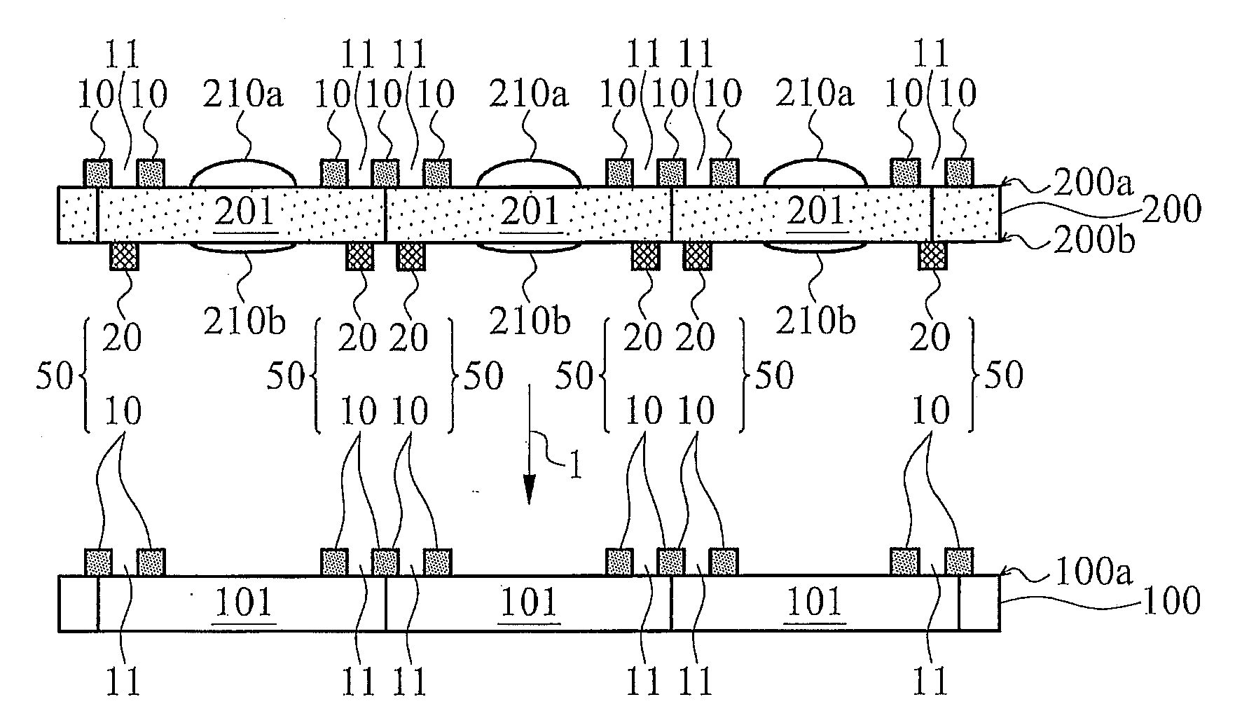
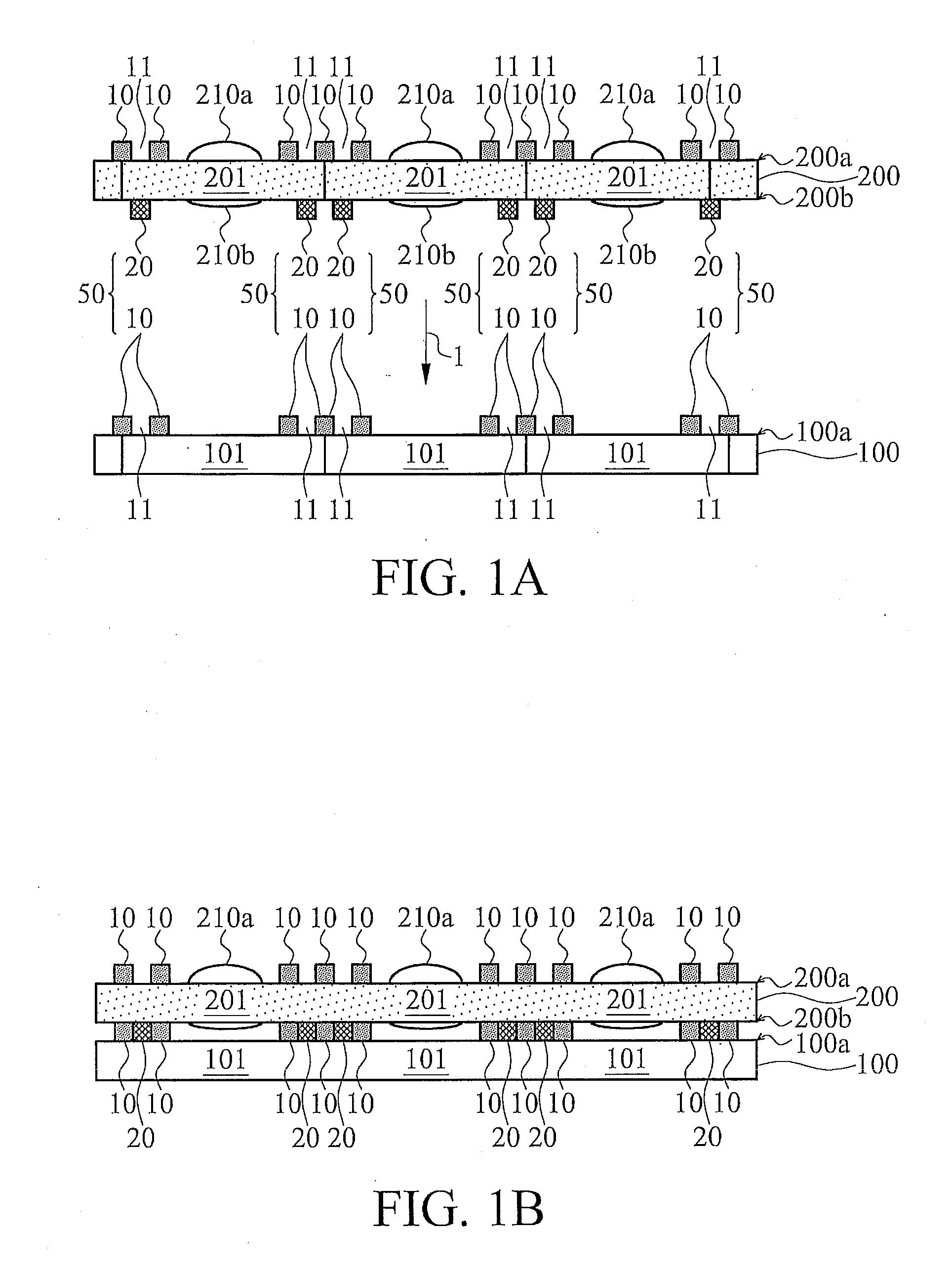
[0024]FIGS. 1A and 1B show cross-sections of an alignment device 50 of a preferred embodiment of the invention and an application thereof. The alignment device 50 comprises a dam structure 10 disposed on a substrate 100 and a post 20 disposed on a substrate 200. The dam structure 10 comprises a groove 11. Exemplary top views of the dam structure 10 and the post 20 are subsequently described. In this embodiment, the substrate 100 is a semiconductor wafer comprising a plurality of chips 101, and the substrate 200 is a lens substrate comprising a plurality of units 201 corresponding to the chips 101.

[0025]In FIG. 1A, the dam structure 10 is disposed on an active surface 1...


PUM


Abstract

An alignment device and applications thereof are disclosed. The device comprises a dam structure disposed on a first substrate, and a post disposed on a second substrate at a position corresponding to the dam structure. The dam structure comprises a groove. The post is disposed in the groove of the dam structure when bonding the first and second substrates.

Description

BACKGROUND OF THE INVENTION[0001]1. Field of the Invention[0002]The invention relates to semiconductor technology and more particularly to a light sensing device.[0003]2. Description of the Related Art[0004]In WO 2004 / 027880 A2, a spacer wafer between two lens wafers to maintain a gap therebetween is disclosed. It is critical to align the substrates because alignment errors therebetween may negatively affect the optical performance of the final light sensing device.[0005]The lenses on the lens wafers are typically formed of transparent polymer cured by illumination of ultraviolet (UV) light or heating. The lens substrates are usually deformed and thus have serious warpage during the lens replication process or substrate bonding process. The spacer and lens substrates typically comprise alignment marks at either side thereof. Due to warpage of the substrates, even if the alignment marks are accurately aligned, and then the substrates are bonded, the corresponding lenses and the space...

Claims


Application Information

Patent Timeline
Patent Type & Authority Applications(United States)
IPC IPC(8): G02B27/10G02B7/00
CPCG02B7/02H01L27/14618H01L27/14625H04N5/2257H01L33/58H04N5/2253H04N5/2254H01L27/14685H01L2924/0002H04N23/57H04N23/54H01L2924/00
Inventor LEE, HSIAO-WEN
Owner VISERA TECH CO LTD
Why Eureka
Try Eureka