Defect inspection method and computer-readable storage medium

a technology of defect inspection and computer-readable storage medium, which is applied in the direction of computing, instruments, measurement devices, etc., can solve the problems of long inability to judge defects on wafers in some cases, so as to reduce the time required for setting the optimum illuminance, shorten the time required for defect inspection, and reduce the effect of tim

Active Publication Date: 2009-09-10
TOKYO ELECTRON LTD
View PDF6 Cites 2 Cited by
  • Summary
  • Abstract
  • Description
  • Claims
  • Application Information

AI Technical Summary

Benefits of technology

[0009]The present invention has been developed in consideration of the above point, and its object is to perform defect inspection of a substrate appropriately in a short time.
[0011]The predetermined luminance means the previously set luminance, and, for example, a luminance in a predetermined range from the luminance of the image obtained by picking up an image of a reference substrate having no defect. For example, when the luminance of the image of the reference substrate is 210, the predetermined luminance is set to, for example, 210±20. Once the image of the luminance at the same level as that of the reference substrate can be obtained as described above, the reference substrate and a substrate to be inspected can be appropriately compared with each other, so that the defects on the substrate can be appropriately judged. Further, when the image of the substrate is brought to have the predetermined luminance, it is avoided that, for example, the image is too bright or too dark to make judgment of defects difficult.
[0013]According to the present invention, since, for setting the optimum illuminance of the illumination, a plurality of measurement regions are set on the substrate, and illuminations at different illuminances are applied to the plurality of measurement regions while the substrate is being moved, to pick up the image of each of the measurement regions, the image of each of the measurement regions can be obtained by a single movement of the substrate. Accordingly, it is unnecessary to move the substrate many times as in the prior art, so that the time required for setting the optimum illuminance can be reduced and therefore the defect inspection can be performed in a short time. Further, since the reference luminances of the images of the measurement regions are found and, based on the correlation between each of the reference luminances and the illuminance, the illuminance at which the reference luminance coincides with the predetermined luminance is set as the optimum illuminance, the optimum illuminance can be automatically set after the images of the measurement regions are obtained. This eliminates the necessity to directly compare the images of the substrate picked up at respective illuminances as in the prior art, so that the defect inspection can be performed in a shorter time. Furthermore, since the image of the substrate illuminated with the illumination at the optimum illuminance is picked up to obtain the image of the substrate, the image of the substrate at the above-described predetermined luminance can be obtained, so that the defects can be appropriately judged from the image of the substrate for inspection.

Problems solved by technology

However, if the luminance of the image of the wafer is too high or too low, defects on the wafer cannot be judged in some cases.
Since it is necessary to move the wafer many times and to pick up the images when the optimum illuminance is set as described above, it has taken a long time to perform the defect inspection.

Method used


Image

  • Defect inspection method and computer-readable storage medium
  • Defect inspection method and computer-readable storage medium
  • Defect inspection method and computer-readable storage medium

Examples


Embodiment Construction

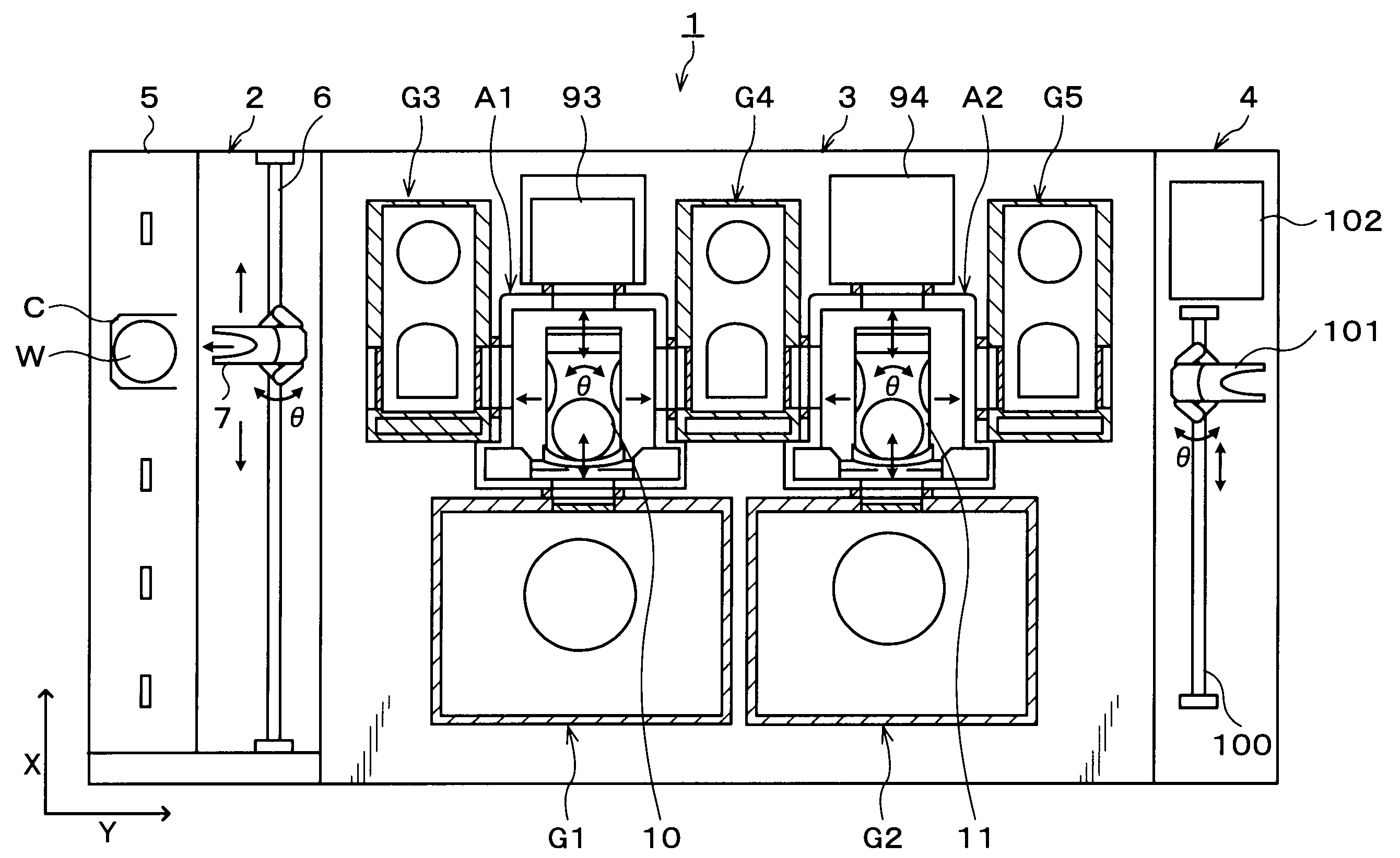
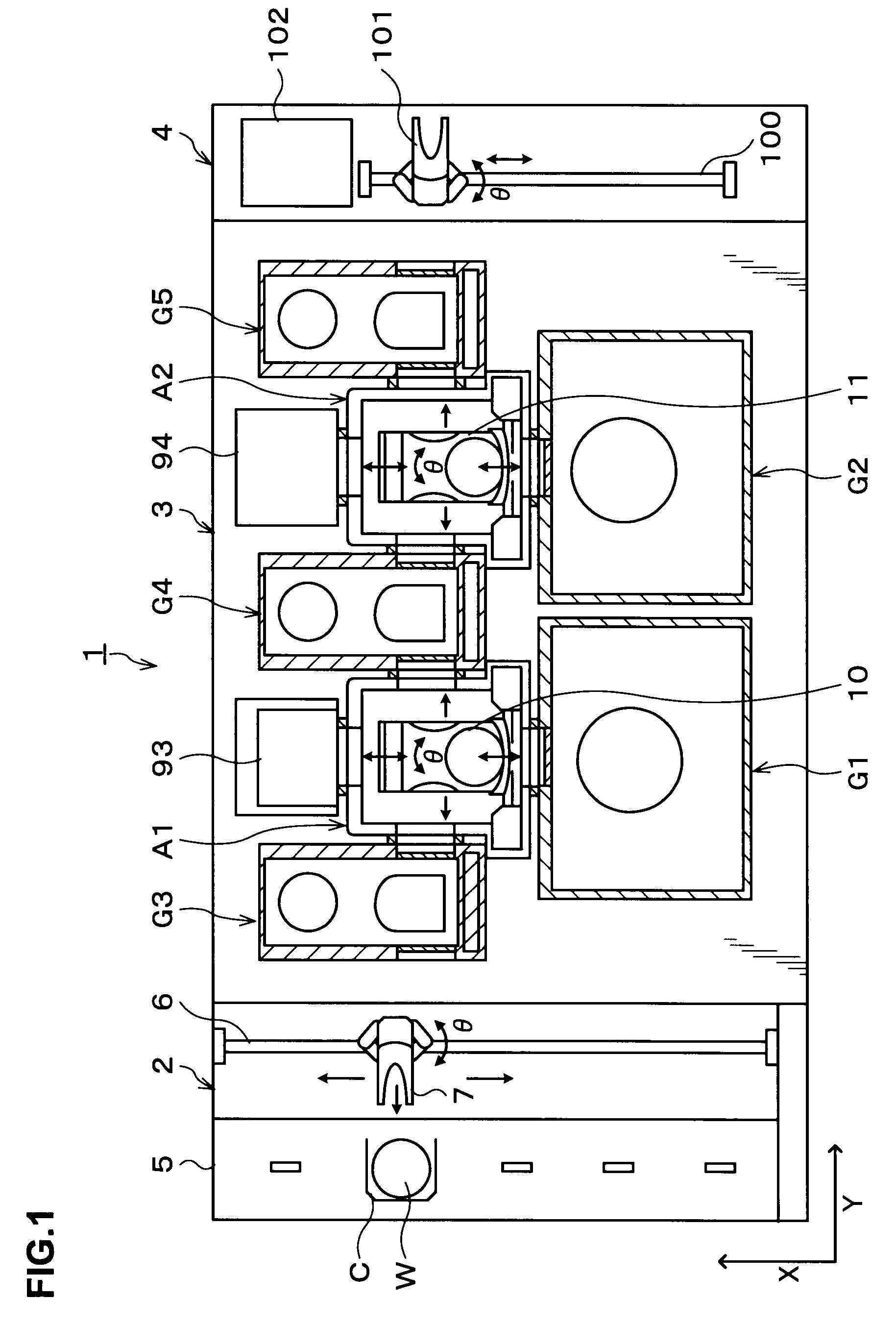
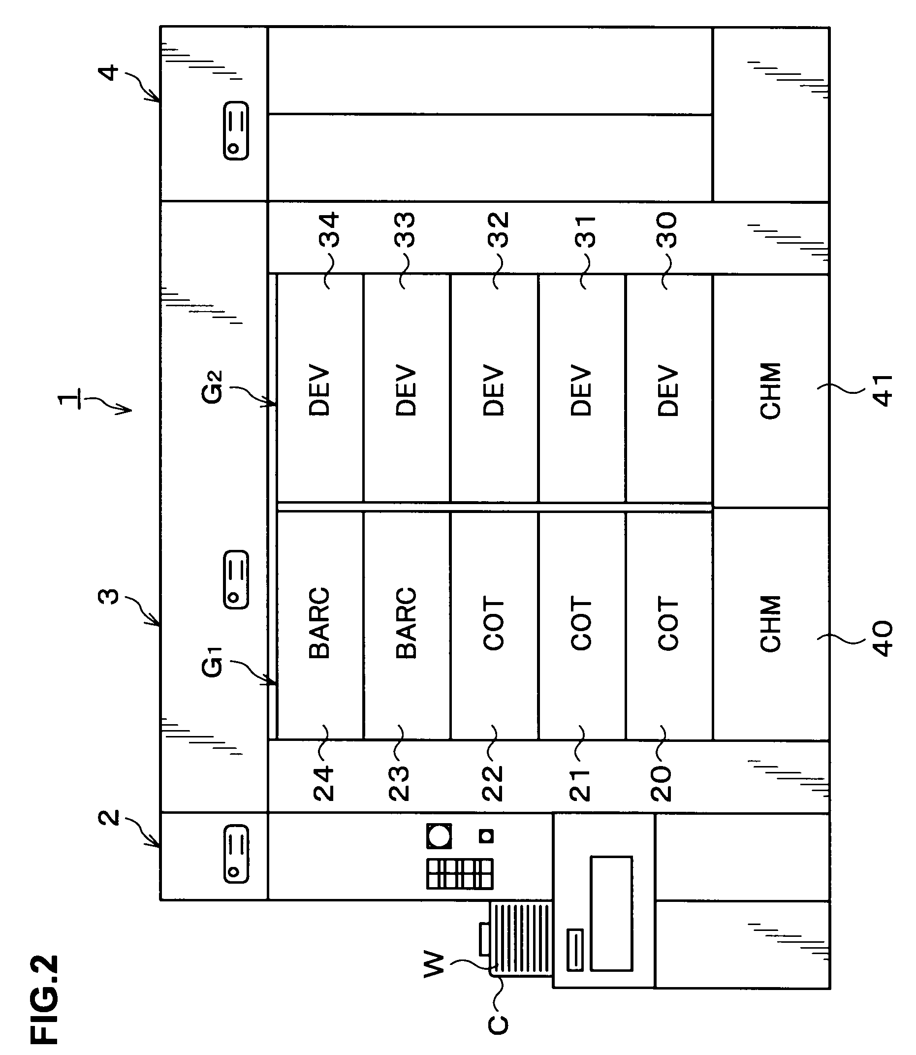
[0028]Hereinafter, preferred embodiments of the present invention will be described. FIG. 1 is a plan view showing the outline of a configuration of a coating and developing treatment system 1 in which a defect inspection unit for implementing a defect inspection method according to the present embodiment is incorporated, FIG. 2 is a front view of the coating and developing treatment system 1, and FIG. 3 is a rear view of the coating and developing treatment system 1.

[0029]The coating and developing treatment system 1 has, as shown in FIG. 1, a configuration in which, for example, a cassette station 2 for transferring, for example, 25 wafers W per cassette as a unit from / to the outside into / from the coating and developing treatment system 1 and transferring the wafers W into / out of a cassette C; a processing station 3 including a plurality of various kinds of processing and treatment units, which are multi-tiered, for performing predetermined processing or treatment in a manner of s...


PUM


Abstract

The present invention includes an illuminance adjustment step of setting an optimum illuminance of the illumination; and a defect inspection step of picking up the image of the substrate illuminated with the illumination at the optimum illuminance, wherein the illuminance adjustment step has: a first step of applying illuminations at different illuminances to a plurality of measurement regions on a front surface of the substrate and picking up an image of each of the measurement regions, while moving the substrate; a second step of making a luminance of the picked up image of each of the measurement regions into a histogram to find a reference luminance where an integral value from a maximum luminance side of the histogram is a predetermined value; and a third step of calculating a correlation between each of the reference luminances and the illuminance, and setting based on the correlation an illuminance at which the reference luminance coincides with a predetermined luminance, as the optimum illuminance.

Description

BACKGROUND OF THE INVENTION[0001]1. Field of the Invention[0002]The present invention relates to a method of picking up an image of a substrate illuminated with illumination to inspect the substrate for defects, and a computer-readable storage medium.[0003]2. Description of the Related Art[0004]In a photolithography processing in manufacture of a semiconductor device, for example, a resist coating treatment of applying a resist solution onto, for example, a semiconductor wafer (hereinafter, referred to as a “wafer”) to form a resist film, exposure processing of exposing a predetermined pattern to light on the resist film, a developing treatment of developing the exposed resist film and so on are performed in sequence to form a predetermined resist pattern on the wafer.[0005]The wafer for which a series of predetermined photolithography processing has been performed is subjected to a so-called macro defect inspection by an inspection apparatus, such as whether or not a predetermined ...

Claims


Application Information

Patent Timeline
Patent Type & Authority Applications(United States)
IPC IPC(8): G06K9/00G06V10/141
CPCG01N21/9501G06K9/2027G01N2021/8835G06V10/141
Inventor HISANO, KAZUYATOMITA, HIROSHINISHIYAMA, TADASHI
Owner TOKYO ELECTRON LTD
Why Eureka
Try Eureka