Heat sink structure and semiconductor package as well as method for configuring heat sinks on a semiconductor package

Inactive Publication Date: 2009-09-17
ADVANCED SEMICON ENG INC
View PDF3 Cites 12 Cited by
  • Summary
  • Abstract
  • Description
  • Claims
  • Application Information

AI Technical Summary

Benefits of technology

[0015]According to the method of the present invention for configuring heat sinks on a semiconductor package, the solder pre-applied on the heat sink acts as a thermal interface material. The heat sink with the solder can be attached to a chip and another heat sink by only a reflow process. The time for configuring the heat sinks on the package can be greatly reduced accordingly. Moreover,

Problems solved by technology

However, it is likely that there will be a lot of voids formed

Method used


Image

  • Heat sink structure and semiconductor package as well as method for configuring heat sinks on a semiconductor package
  • Heat sink structure and semiconductor package as well as method for configuring heat sinks on a semiconductor package
  • Heat sink structure and semiconductor package as well as method for configuring heat sinks on a semiconductor package

Examples


Example

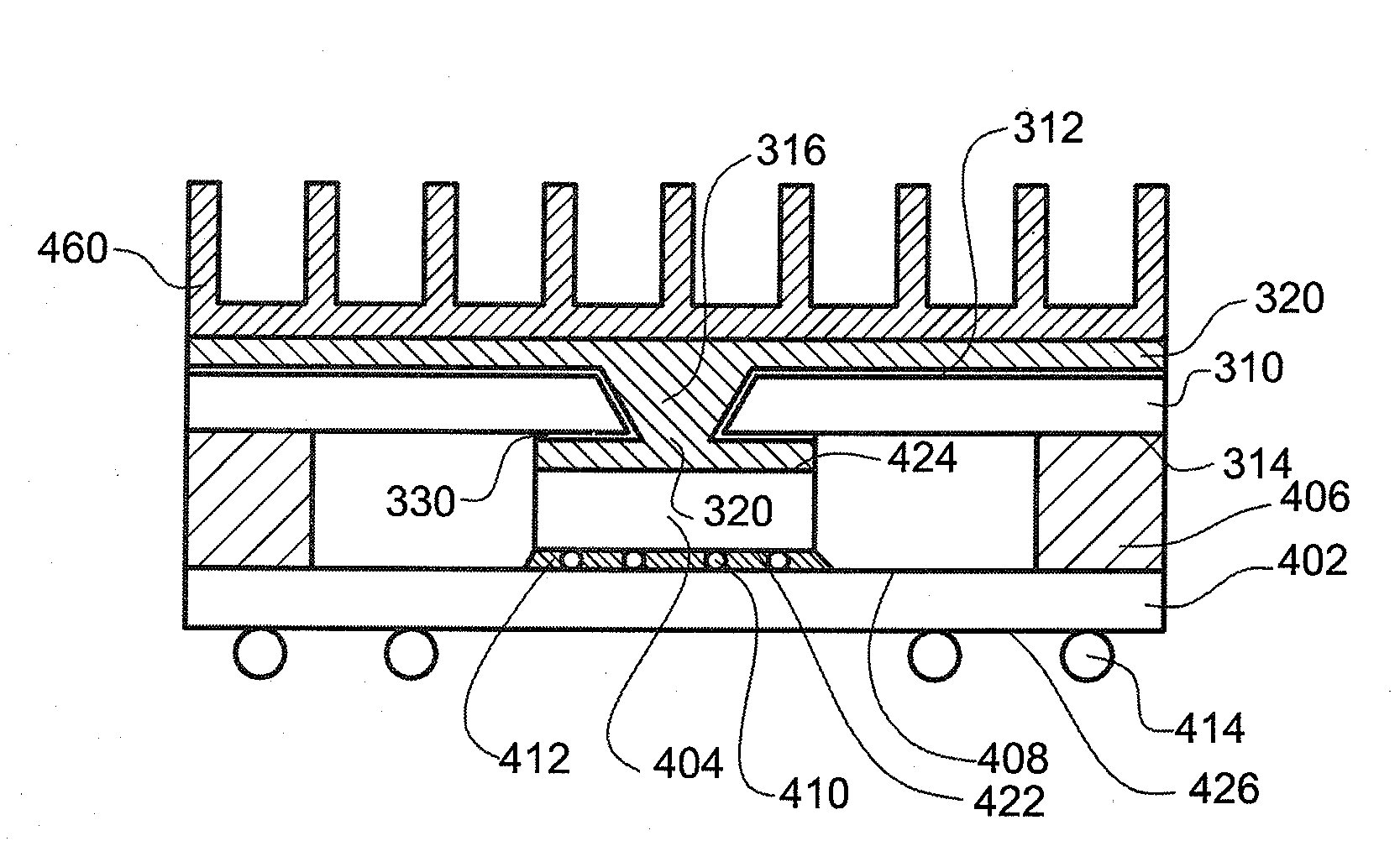
[0024]Referring to FIGS. 6a and 6c, the heat sink structure 300 according to the present invention includes a heat sink 310 that has a through opening 316 extending from the upper surface 312 through to the lower surface 314. A solder 320 as a metal interface material, made of such as indium, silver, lead or alloys thereof is disposed in the through opening 316 and on the lower surface 314 of the heat sink 310. Moreover, the solder 320 can be further disposed on full or part of the upper surface 312, wherein the portion of the solder 320 in the through opening 316 is connected with the portions of the solder on the upper and lower surfaces 312, 314. The inner wall of the through opening 316 and the portions of the upper and lower surfaces 312, 314 in contact with the solder 320 can be optionally coated with a layer of Au or Ni / Au material 330.

[0025]Referring to FIGS. 7a and 7b, they illustrate the method for configuring heat sinks on a semiconductor package according to the present ...


PUM


Abstract

A heat sink structure according to the present invention is provided. The heat sink has a through opening extending from the upper surface through to the lower surface. A solder is disposed in the through opening and on the upper and lower surfaces of the heat sink, wherein the portion of the solder in the through opening is connected with the portions of the solder on the upper and lower surfaces.

Description

CROSS REFERENCE TO RELATED APPLICATION[0001]This application claims the priority benefit of Taiwan Patent Application Serial Number 097108438 filed Mar. 11, 2008, the full disclosure of which is incorporated herein by reference.BACKGROUND OF THE INVENTION[0002]1. Field of the Invention[0003]The invention relates to a heat sink structure, a semiconductor package and a method for configuring heat sinks on a semiconductor package and more particularly, to a heat sink structure pre-applied with a layer of solder, a semiconductor package with the above heat sink structure and a method for configuring the above heat sink structure on a semiconductor package.[0004]2. Description of the Related Art[0005]High-performance flip chip ball grid array (HFCBGA) package is one of the reinforced packages that has a metal ring to support a heat sink for covering the package. Referring to FIG. 1, a conventional HBCBGA package 100 includes a substrate 102, a chip 104 disposed on the upper surface 108 o...

Claims


Application Information

Patent Timeline
IPC IPC(8): H01L23/367H01L21/56F28F7/00
CPCH01L23/3736H01L23/42H01L2224/16H01L2924/16195H01L2924/01079H01L2924/15311H01L2224/73253
Inventor WANG, TONG HONGLEE, CHANG CHI
Owner ADVANCED SEMICON ENG INC
Why Eureka
Try Eureka