Chip structure and stacked chip package as well as method for manufacturing chip structures

Inactive Publication Date: 2009-09-17
ADVANCED SEMICON ENG INC
View PDF4 Cites 3 Cited by
  • Summary
  • Abstract
  • Description
  • Claims
  • Application Information

AI Technical Summary

Benefits of technology

[0009]It is an object of the present invention to provide a chip structure that can be stacked on another chip without need of an additional spacer or dummy chip to maintain a gap between the two chips for wire bonding.

Problems solved by technology

However, the above stacked chips with organic or inorganic spacers all are manufactured with more complicated process.

Method used


Image

  • Chip structure and stacked chip package as well as method for manufacturing chip structures
  • Chip structure and stacked chip package as well as method for manufacturing chip structures
  • Chip structure and stacked chip package as well as method for manufacturing chip structures

Examples


Embodiment Construction

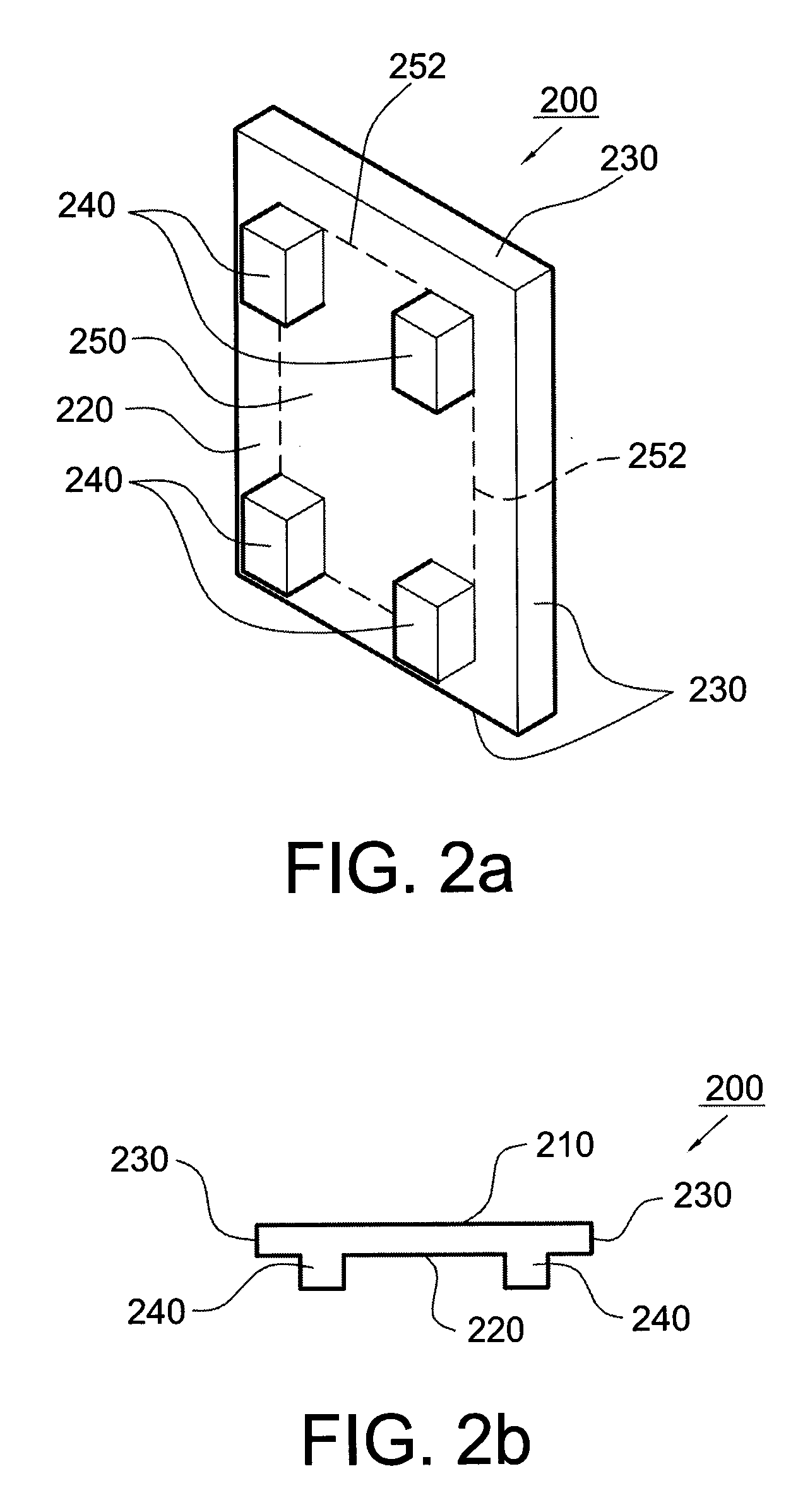
[0023]Referring to FIGS. 2a, 2b and 2c, the chip structure 200 according to the present invention includes an active surface 210, a back surface 220 opposing to the active surface 210 and a plurality side surfaces 230 extending from the active surface 210 to the back surface 220. A rectangular area 250 is defined on the back surface 220 of the chip structure 200. The area 250 has four sides 252, each of the sides 252 is parallel to and away from one of the side surfaces 230 for a non-zero distance. The chip structure 200 further includes a plurality of pedestals 240 perpendicularly extending from the back surface 220. The pedestals 240 can be four rectangular pedestals respectively disposed on the four corners of the area 250. Specifically, the each pedestal 240 is disposed away from the nearest side surface 230 for a non-zero distance.

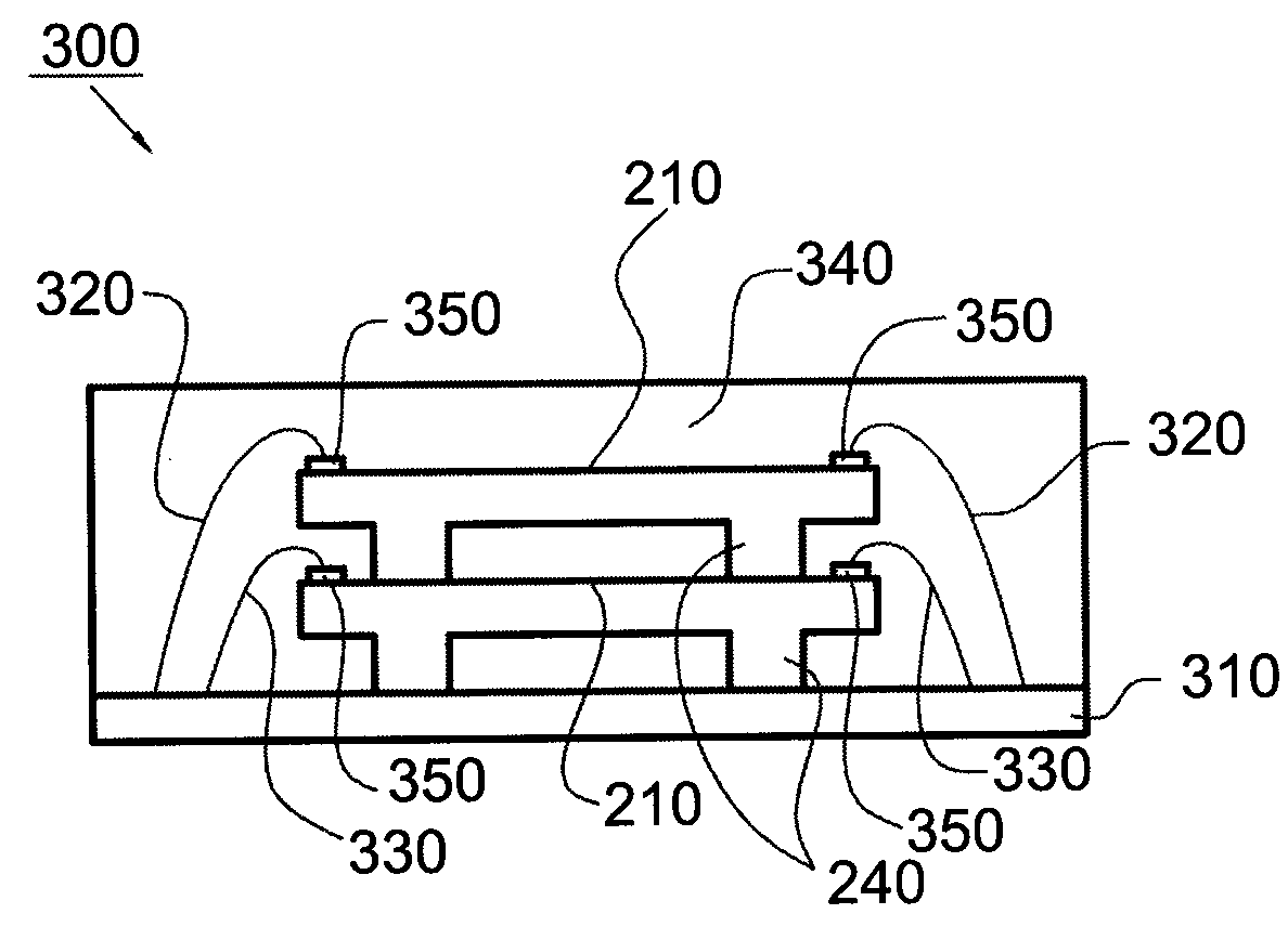
[0024]Referring to FIG. 3, the stacked chip package 300 according to the present invention includes two chip structures 200, one of which is the lowe...


PUM


Abstract

A chip structure according to the present invention is provided. A plurality of pedestals extends from the back surface of the chip structure. Each of the pedestals is located at a position away from the edge of the back surface for a non-zero distance so that the pedestals of an upper chip structure will not damage the bonding pads positioned on the edge of the active surface of a lower chip structure when the upper chip structure is stacked on the active surface of the lower chip structure with the pedestals.

Description

CROSS REFERENCE TO RELATED APPLICATION[0001]This application claims the priority benefit of Taiwan Patent Application Serial Number 097108439 filed Mar. 11, 2008, the full disclosure of which is incorporated herein by reference.BACKGROUND OF THE INVENTION[0002]1. Field of the Invention[0003]The invention relates to a chip structure, a stacked chip package and a method for manufacturing chip structures and more particularly, to a chip structure with pedestals, a stacked chip package with the above chip structure and a method for manufacturing chip structures with pedestals.[0004]2. Description of the Related Art[0005]In the electronics industry, as products become smaller and smaller, increased miniaturization of integrated circuit (IC) packages has become more and more critical. At the same time, higher performance and lower cost have become essential for new products.[0006]In order to put more integrated circuit chips in a single package to reduce the profile of the product, the ma...

Claims


Application Information

Patent Timeline
Patent Type & Authority Applications(United States)
IPC IPC(8): H01L23/49H01L21/304
CPCH01L21/6835H01L2224/85H01L21/78H01L24/26H01L24/83H01L24/85H01L24/96H01L25/0657H01L29/0657H01L2221/68327H01L2224/48091H01L2224/48227H01L2224/8385H01L2225/0651H01L2225/06555H01L2225/06575H01L2924/07802H01L2924/10158H01L2924/14H01L21/6836H01L2924/01033H01L2924/00014H01L2924/181H01L2924/10155H01L24/48H01L2924/00012H01L2224/45015H01L2924/207H01L2224/45099
Inventor TSAI, TSUNG YUEHLAI, YI SHAOHUANG, CHENG WEI
Owner ADVANCED SEMICON ENG INC
Why Eureka
Try Eureka