Light emitting device using electron emission and flat display apparatus using the same

a technology of light emitting devices and flat display devices, which is applied in the direction of instruments, discharge tubes, luminescnet screens, etc., can solve the problems of low luminous efficiency, high driving voltage and low luminous efficiency, and light emitting devices have a quick response tim

Inactive Publication Date: 2007-04-12
SAMSUNG SDI CO LTD
View PDF8 Cites 11 Cited by
  • Summary
  • Abstract
  • Description
  • Claims
  • Application Information

AI Technical Summary

Benefits of technology

[0014] The device may further include: a substrate supporting the anode electrode and the phosphor layer; and a spacer maintaining a gap between the PN junction and the substrate.
[0015] Alternatively, the device may further include: a first substrate on which the PN junctions are formed; a second substrate supporting the anode electrode and the phosphor layer; and a spacer maintaining a gap between the first substrate and the second substrate.

Problems solved by technology

However, conventional PDPs and flat lamps operated by plasma discharge require sufficiently high energy to ionize the discharge gas, and thus, have a high driving voltage and low luminous efficiency.
In addition, SCE type light emitting devices have a quick response time, which is one of the drawbacks of liquid crystal displays (LCDs), and do not produce residual images, even when there is fast motion, as in, for example, sports programs.
Further, since SCE type light emitting devices generally have low power consumption, they are receiving a lot of attention as next-generation displays.
However, a conventional method of forming a nano-sized gap has problems in terms of repeatability and / or reliability.

Method used


Image

  • Light emitting device using electron emission and flat display apparatus using the same
  • Light emitting device using electron emission and flat display apparatus using the same
  • Light emitting device using electron emission and flat display apparatus using the same

Examples


first embodiment

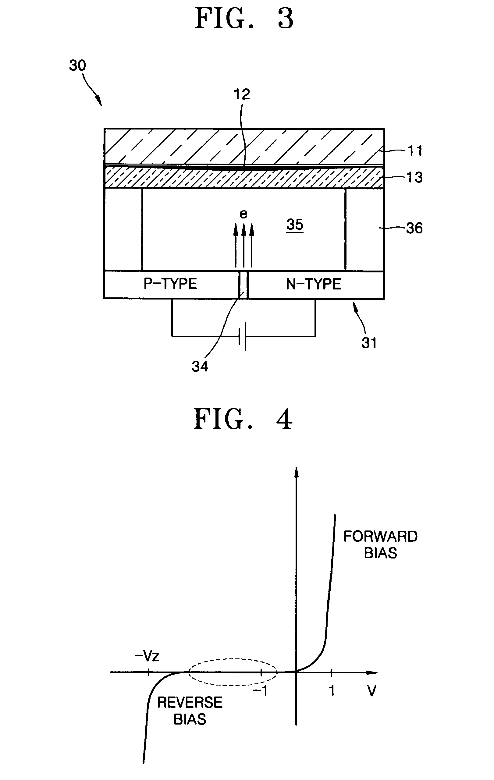
[0033]FIG. 3 is a schematic cross-sectional view of a light emitting device 30 using electron emission according to a FIG. 4 is a graph illustrating current characteristics of a PN junction 31 used in the light emitting device 30 of FIG. 3.

[0034] Referring to FIG. 3, the light emitting device 30 includes the PN junction 31, an anode electrode 12, and a phosphor layer 13.

[0035] The PN junction 31 includes a depletion layer 34 having a predetermined thickness in an area where a p-type semiconductor and an n-type semiconductor are bonded. The anode electrode 12 faces the depletion layer 34 and is separated from the depletion layer 34 by a predetermined distance. The phosphor layer 13 is attached to a surface of the anode electrode 12. The thickness of the depletion layer 34 may be from about 1 nm to about 100 nm.

[0036] The light emitting device 30 may further include a substrate 11 on which the anode electrode 12 and the phosphor layer 13 are sequentially formed. The PN junction 31 ...

second embodiment

[0045]FIG. 5 is a schematic cross-sectional view of a light emitting device 130 using electron emission according to a

[0046] Referring to FIG. 5, the light emitting device 130 includes a plurality of PN junctions 131, an anode electrode 12, and a phosphor layer 13. The light emitting device 130 may further include a first substrate 37 on which the PN junctions 37 are formed, a second substrate 11 on which the anode electrode 12 and the phosphor layer 13 are sequentially formed, and a plurality of spacers (not shown) which maintain the space 35 between the first substrate 37 and the second substrate 11. The first substrate 37 and the second substrate 11 may be sealed with glass frit. The light emitting device 130 can also generate visible light using the two methods described above.

third embodiment

[0047]FIG. 6 is a schematic cross-sectional view of a light emitting device 230 using electron emission according to a

[0048] Referring to FIG. 6, the light emitting device 230 includes a monocrystalline substrate 231, an anode electrode 12, and a phosphor layer 13. The entirety of the monocrystalline substrate 231 is doped with p-type impurities, and PN junctions are formed on a surface of the monocrystalline substrate 231. The PN junctions each include a depletion layer 234 having a predetermined thickness, and the depletion layer 233 is formed by diffusing n-type impurities 232 into the surface of the monocrystalline substrate 231. The anode electrode 12 is opposite the monocrystalline substrate 231, and the phosphor layer 13 is attached to a surface of the anode electrode 12. The light emitting device 230 may further include a front substrate 11 on which the anode electrode 12 and the phosphor layer 13 are sequentially formed, and the thickness of the depletion layer 233 may be f...


PUM

PropertyMeasurementUnit
thicknessaaaaaaaaaa
pressureaaaaaaaaaa
thicknessaaaaaaaaaa

Abstract

Provided are a light emitting device using electron emission with a low driving voltage and high luminous efficiency, and a flat display apparatus using the light emitting device. In addition, a light emitting device using electron emission in which with a nano-sized gap can be formed with repeatability and have reliability is provided. The light emitting device includes: a plurality of PN junctions, each including a depletion layer having a predetermined thickness; an anode electrode facing the depletion layer and separated from the depletion layer by a predetermined distance; and a phosphor layer formed on a surface of the anode electrode. The flat display apparatus includes the light emitting device.

Description

CROSS-REFERENCE TO RELATED PATENT APPLICATION [0001] This application claims the benefit of Korean Patent Application No. 10-2005-0095487, filed on Oct. 11, 2005, in the Korean Intellectual Property Office, the disclosure of which is incorporated herein in its entirety by reference. BACKGROUND OF THE INVENTION [0002] 1. Field of the Invention [0003] The present embodiments relate to a light emitting device using electron emission and a flat display apparatus using the same, and more particularly, to a light emitting device using electron emission which has a low driving voltage and high luminous efficiency, and a flat display apparatus using the light emitting device. [0004] 2. Description of the Related Art [0005] A plasma display panel (PDP), which is a flat display apparatus, forms an image using an electrical discharge. Due to their superior display properties such as high brightness and large viewing angle, PDPs are widely used. PDPs may be classified as facing discharge type o...

Claims


Application Information

Patent Timeline
Patent Type & Authority Applications(United States)
IPC IPC(8): H01J1/62H01J63/04F21S2/00F21Y101/00F21Y105/00G02F1/13357H01J63/06H01J63/08
CPCG02F1/133602G02F2001/133625H01J1/308H01J29/481H01J31/127H01J63/02H01J63/08G02F1/133625H01J1/63
Inventor SON, SEUNG-HYUNKIM, GI-YOUNG
Owner SAMSUNG SDI CO LTD
Why Eureka
Try Eureka