Photo-sensing device, photosensor, and display device

Inactive Publication Date: 2009-09-24
CASIO COMPUTER CO LTD
View PDF7 Cites 10 Cited by
  • Summary
  • Abstract
  • Description
  • Claims
  • Application Information

AI Technical Summary

Benefits of technology

[0017]Accordingly, the object of the present invention is to provide a photo-sensing device having high sensitivity to an incident light and capable to be made compact, a photosensor, and a display device.
[0024]According to present invention, large output current can be obtained, and the sensitivity to incident light can be enhanced while compactness is maintained.

Problems solved by technology

The photocurrent obtained through a conventional thin-film phototransistor 80 is limited, which is why it is difficult to detect low illuminance accurately.

Method used


Image

  • Photo-sensing device, photosensor, and display device
  • Photo-sensing device, photosensor, and display device
  • Photo-sensing device, photosensor, and display device

Examples


Embodiment Construction

[0061]Hereinafter, various embodiments of the present invention will be described in detail with reference to the figures in which like reference characters are used to designate like or corresponding components.

(Photo-Sensing Device)

[0062]A photo-sensing device of the present invention will be described first.

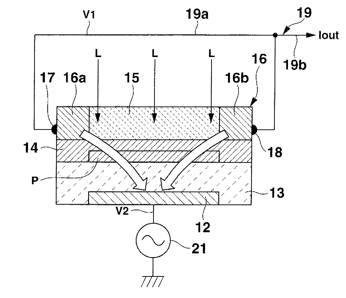
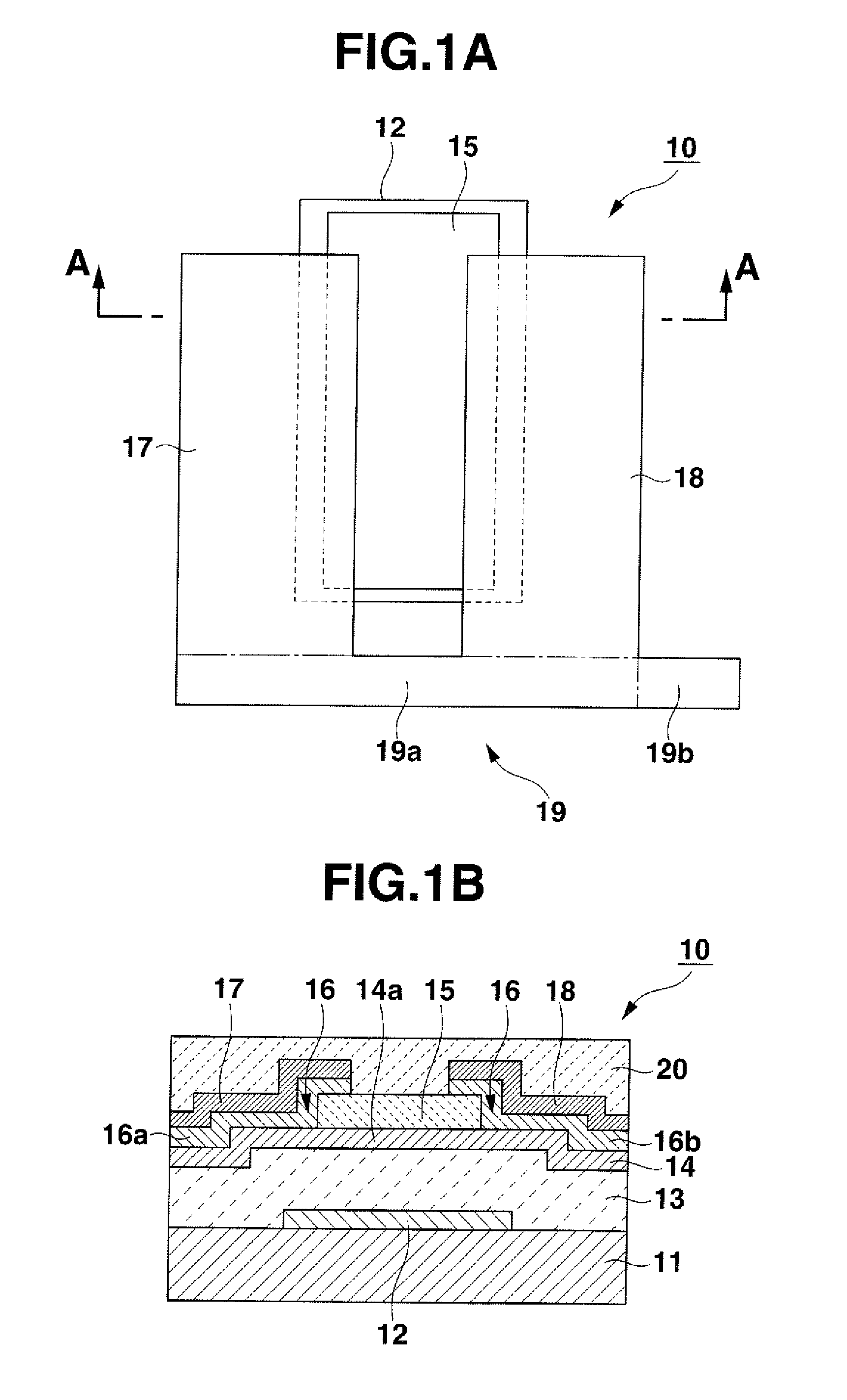
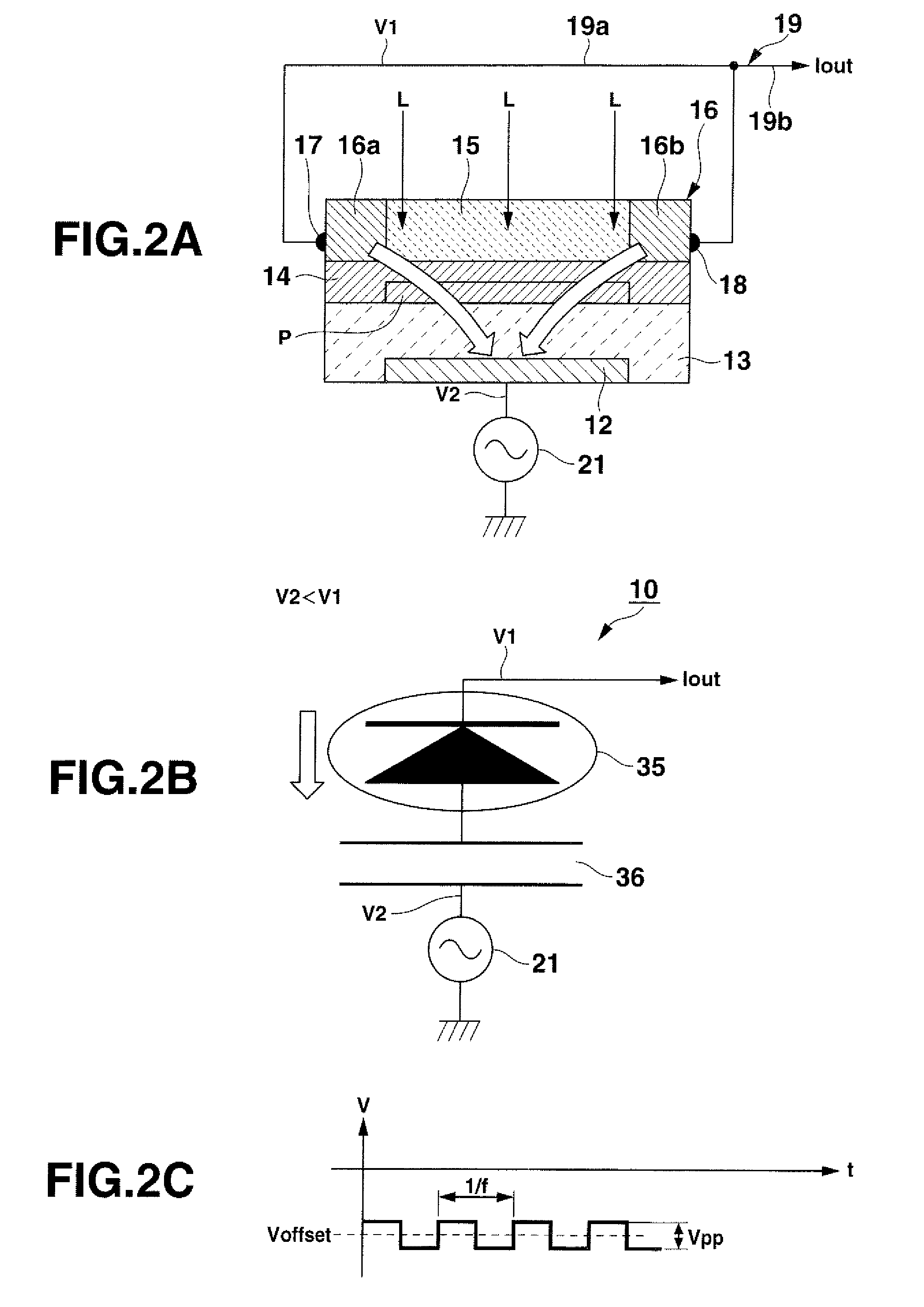
[0063]FIG. 1A is a perspective plan view illustrating a partial construction of a photo-sensing device 10, and FIG. 1B is a cross-sectional view of the photo-sensing device in FIG. 1A taken along a line A-A.

[0064]As shown in FIG. 1B, a photo-sensing device 10 is comprised of a substrate 11, and following layers are provided onto the substrate 11 in order: a first electrode 12 on the lower side, an insulating film 13, a photoelectric conversion semiconductor thin film 14, an optical sensing region passivation film 15, a first and a second low resistance semiconductor thin films 16a and 16b, electrodes for the first and the second low resistance semiconductor thin films 17 and 1...


PUM


Abstract

A photo-sensing device is disclosed, comprising a photoelectric conversion semiconductor thin film, thin films for ohmic contacts to be provided to form an incident light window on one face of the photoelectric conversion semiconductor thin film, first and second ohmic electrodes installed on the thin films for the ohmic contacts, a connection wiring for short-circuiting the first and the second ohmic electrodes, an insulating film provided on the other face of the photoelectric conversion semiconductor thin film, and a first electrode provided on the face of the insulating film that does not contact the photoelectric conversion semiconductor thin film.

Description

[0001]This application claims the benefit of Japanese Application No. JP 2008-076880 filed, in Japan on Mar. 24, 2008, of which is hereby incorporated by reference in this entirety.BACKGROUND OF THE INVENTION[0002]1. Field of the Invention[0003]The present invention relates to a photo-sensing device, a photosensor and a display device.[0004]2. Description of the Related Art[0005]Thin-film phototransistors featuring thin-film transistors (TFTs) are well known.[0006]FIGS. 17A and 17B show a typical structure of a conventional thin-film phototransistor 80. FIG. 17A is a perspective plan view illustrating the structure of a conventional thin-film phototransistor 80. FIG. 17B is a cross-sectional view of the phototransistor in FIG. 17A taken along a line D-D. The thin-film phototransistor 80, which has the same structure as a TFT installed in the pixel display part of a TFT liquid crystal display, is configured as an amorphous silicon (a-Si) TFT. The thin-film phototransistor 80 includes...

Claims


Application Information

Patent Timeline
IPC IPC(8): H01L31/00H01L31/10
CPCG09G3/3406G09G3/36G09G2320/0242G09G2320/0626G09G2360/144G09G2360/145H01L27/14603H01L2924/0002H01L27/14692H01L31/105H01L31/1136H01L2924/00
Inventor YAMAGUCHI, IKUHIRO
Owner CASIO COMPUTER CO LTD
Why Eureka
Try Eureka