Methods of Forming Metal Interconnect Structures on Semiconductor Substrates Using Oxygen-Removing Plasmas and Interconnect Structures Formed Thereby

Active Publication Date: 2009-09-24
IBM CORP +2
View PDF30 Cites 10 Cited by
  • Summary
  • Abstract
  • Description
  • Claims
  • Application Information

AI Technical Summary

Problems solved by technology

A copper oxide film may be formed because it is difficult to completely intercept oxygen during the CMP process, and slurries used in the CMP process typically contain oxygen components.
If a copper oxide film exists on the copper interconnection, the adhesion of the copper connection to a layer deposited on the copper interconnection may be degraded, and the interconnection resistance may be increased, thereby deteriorating the reliability of the semiconductor device.
Accordingly, when a plasma process is performed with respect to the insulating layer formed of a low-k material, the porosity of the insulating layer may be further increased if carbon is removed therefrom, and this increase in porosity may decrease the reliability of the semiconductor device.
However, as the plasma process is performed for a longer time, the thickness of the insulating layer being damaged by carbon removal becomes greater.
If the thickness of the damaged insulating layer is increased, then electron movement therein may occur and cause current leakage to neighboring interconnections.
The porosity of the insulating layer may also be increased and thereby shorten the lifetime of the device.
However, if the plasma process is weakly performed in order to reduce the thickness of the damaged insulating layer, the copper oxide layer may not be completely removed.

Method used

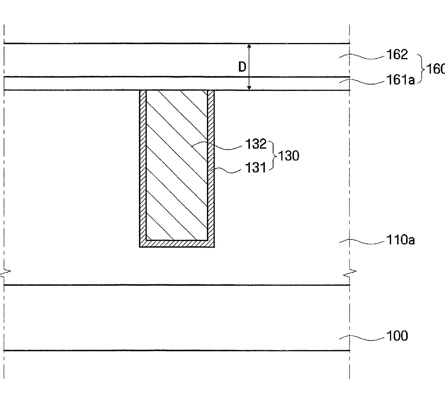
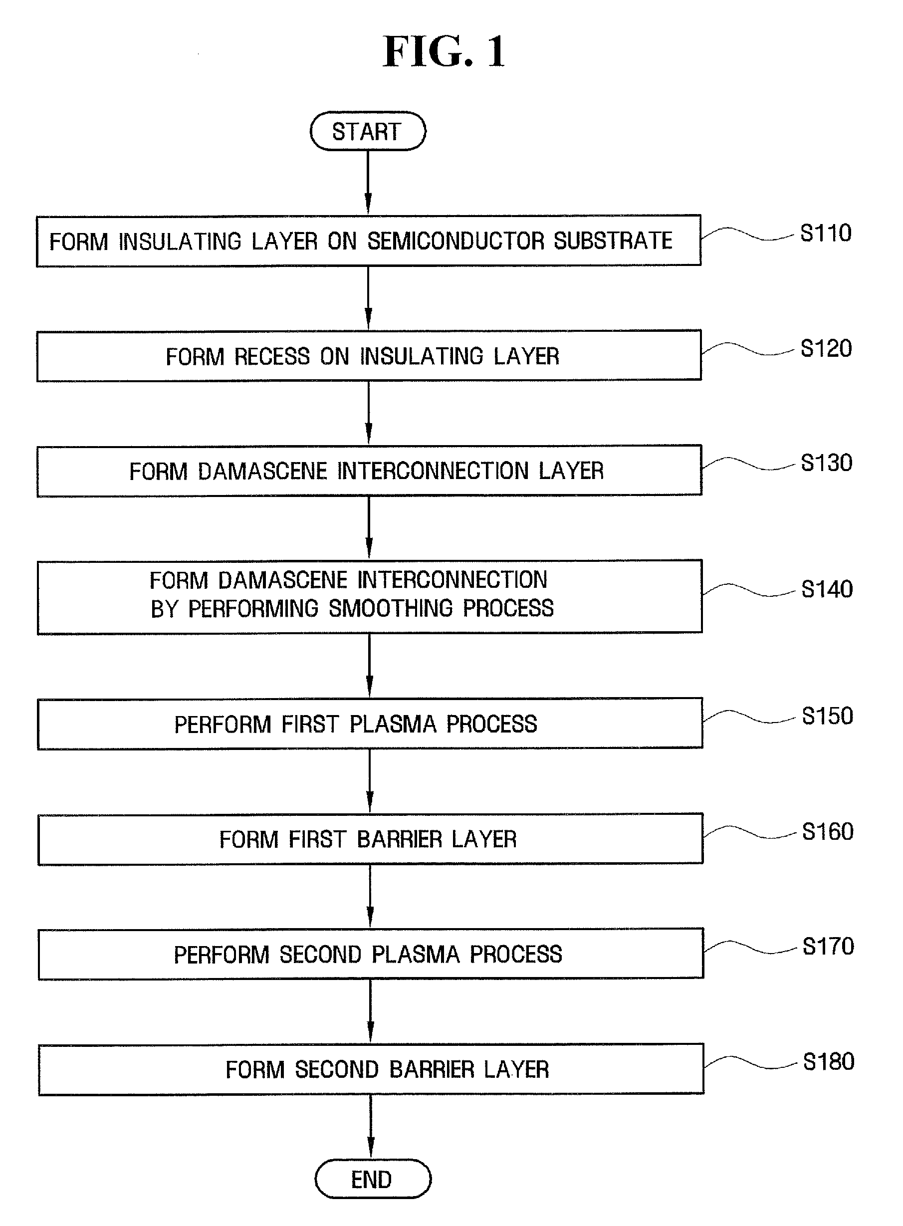
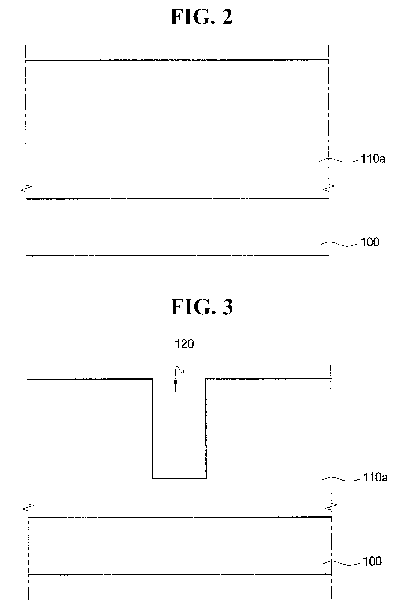

Image

  • Methods of Forming Metal Interconnect Structures on Semiconductor Substrates Using Oxygen-Removing Plasmas and Interconnect Structures Formed Thereby
  • Methods of Forming Metal Interconnect Structures on Semiconductor Substrates Using Oxygen-Removing Plasmas and Interconnect Structures Formed Thereby
  • Methods of Forming Metal Interconnect Structures on Semiconductor Substrates Using Oxygen-Removing Plasmas and Interconnect Structures Formed Thereby

Examples


Embodiment Construction

[0014]The present invention is described more fully hereinafter with reference to the accompanying drawings, in which embodiments of the invention are shown. This invention may, however, be embodied in many different forms and should not be construed as limited to the embodiments set forth herein. Rather, these embodiments are provided so that this disclosure will be thorough and complete, and will fully convey the scope of the invention to those skilled in the art. In the drawings, the sizes and relative sizes of layers and regions may be exaggerated for clarity.

[0015]It will be understood that when an element or layer is referred to as being “on,”“connected to” or “coupled to” another element or layer (and variants thereof), it can be directly on, connected or coupled to the other element or layer or intervening elements or layers may be present. In contrast, when an element is referred to as being “directly on,”“directly connected to” or “directly coupled to” another element or l...


PUM


Abstract

Methods of forming devices include forming a first electrically insulating layer having a metal interconnection therein, on a substrate and then forming a first electrically insulating barrier layer on an upper surface of the metal interconnection and on the first electrically insulating layer. The first electrically insulating barrier layer is exposed to a plasma that penetrates the first electrically insulating barrier and removes oxygen from an upper surface of the metal interconnection. The barrier layer may have a thickness in a range from about 5 Å to about 50 Å and the plasma may be a hydrogen-containing plasma that converts oxygen on the upper surface of the metal interconnection to water.

Description

FIELD OF THE INVENTION[0001]The present invention relates to semiconductor device fabrication methods and, more particularly, to methods of forming semiconductor devices with copper interconnects therein.BACKGROUND OF THE INVENTION[0002]Copper (Cu) has been used as an interconnection material in order to reduce the resistance of interconnections. In the case of forming a copper interconnection, a damascene process is generally used. In the damascene process, chemical mechanical polishing (CMP) may be performed, and after the CMP process is performed, a thin copper oxide film may be formed on the copper interconnection. A copper oxide film may be formed because it is difficult to completely intercept oxygen during the CMP process, and slurries used in the CMP process typically contain oxygen components. If a copper oxide film exists on the copper interconnection, the adhesion of the copper connection to a layer deposited on the copper interconnection may be degraded, and the intercon...

Claims


Application Information

Patent Timeline
IPC IPC(8): H01L21/4763
CPCH01L21/76826H01L21/76829H01L21/76832H01L21/76876H01L21/76883H01L2924/0002H01L23/53233H01L2924/00H01L21/304H01L21/28
Inventor KIM, JAE HAKBONILLA, GRISELDAMOLIS, STEVEN E.RESTAINO, DARRYL D.SHOBHA, HOSADURGAWIDODO, JOHNNY
Owner IBM CORP
Why Eureka
Try Eureka