Multi-Level Striping and Truncation Channel-Equalization for Flash-Memory System

a flash memory and multi-level striping technology, applied in the direction of memory adressing/allocation/relocation, instruments, coding, etc., can solve the problems of mlc flash performance, reliability and durability may decrease, and the nand flash has limitations

Inactive Publication Date: 2009-09-24
SUPER TALENT TECH CORP
View PDF27 Cites 387 Cited by
  • Summary
  • Abstract
  • Description
  • Claims
  • Application Information

AI Technical Summary

Problems solved by technology

However, NAND flash has limitations.
One limitation of NAND flash is that when storing data (writing to flash), the flash can only write from ones (1) to zeros (0).
Another limitation is that NAND flash memory has a finite number of erase cycles between 10,000 and 100,000, after which the flash wears out and becomes unreliable.
But the performance, reliability and durability may decrease for MLC flash.
A similar problem could occur with other bus protocols, such as Serial AT-Attachment (SATA), integrated device electronics (IDE), Serial small-computer system interface (SCSI) (SAS) bus, a fiber-channel ...

Method used


Image

  • Multi-Level Striping and Truncation Channel-Equalization for Flash-Memory System
  • Multi-Level Striping and Truncation Channel-Equalization for Flash-Memory System
  • Multi-Level Striping and Truncation Channel-Equalization for Flash-Memory System

Examples


Embodiment Construction

[0046]The present invention relates to an improvement in Multi-Level Flash Memory Systems. The following description is presented to enable one of ordinary skill in the art to make and use the invention as provided in the context of a particular application and its requirements. Various modifications to the preferred embodiment will be apparent to those with skill in the art, and the general principles defined herein may be applied to other embodiments. Therefore, the present invention is not intended to be limited to the particular embodiments shown and described, but is to be accorded the widest scope consistent with the principles and novel features herein disclosed.

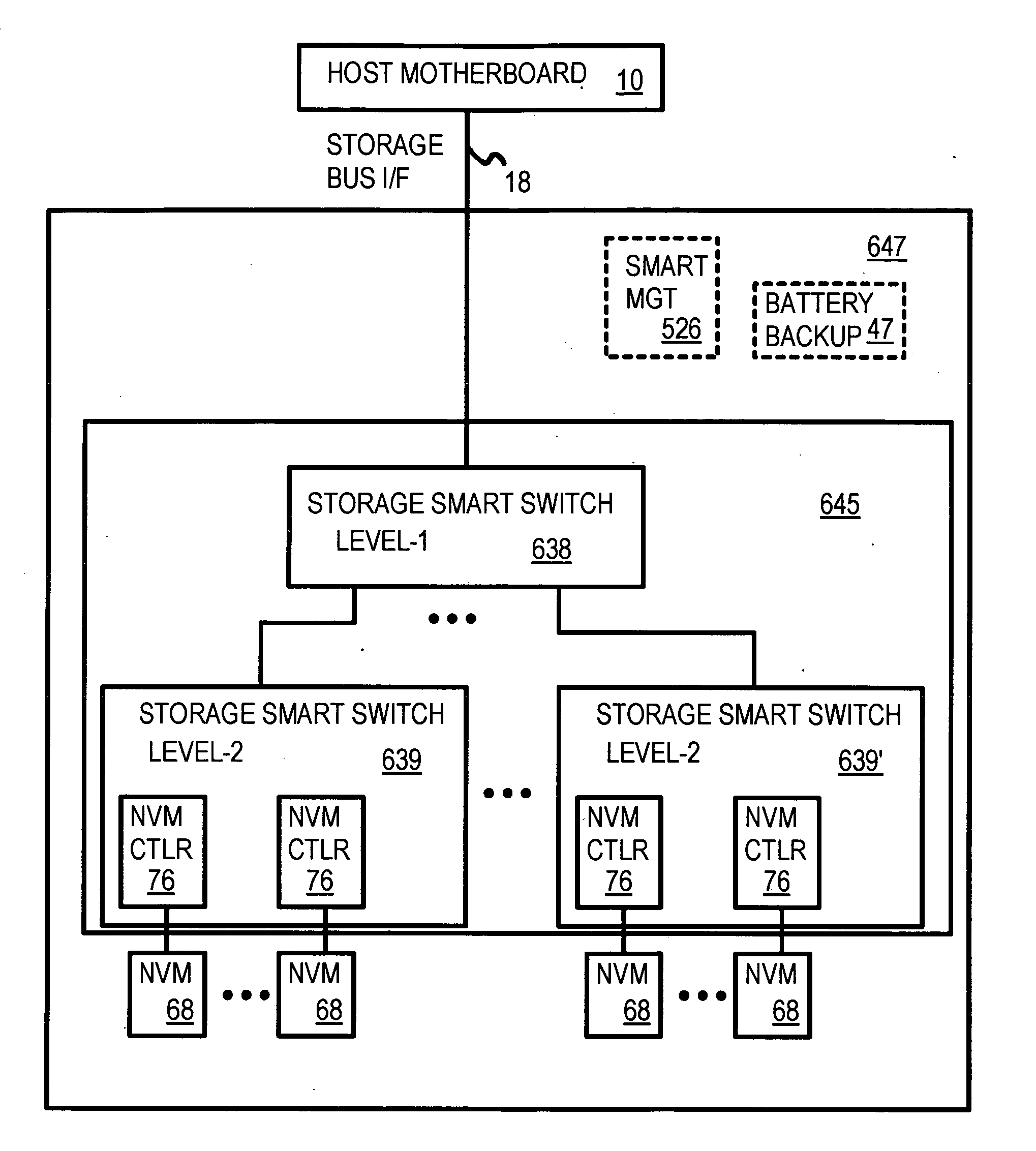
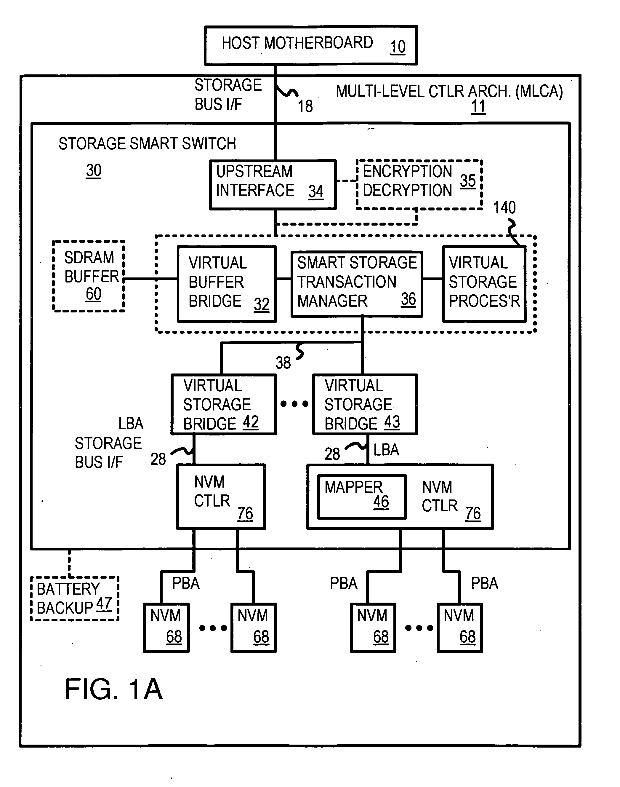
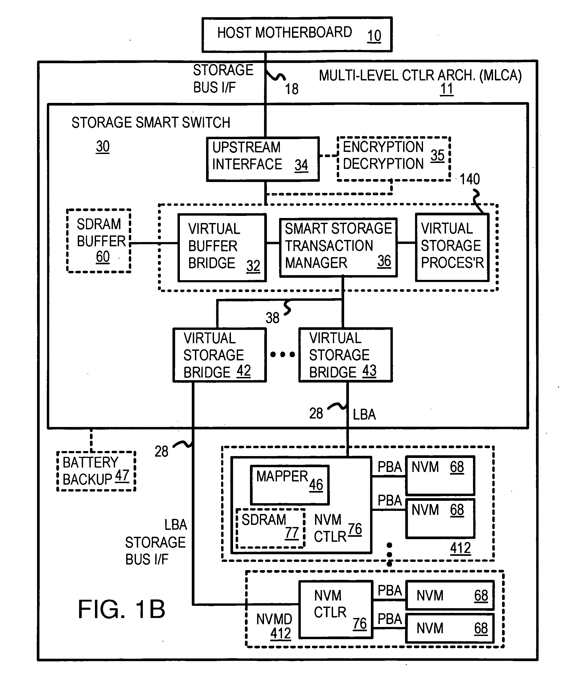
[0047]FIG. 1A shows a smart storage switch using hybrid flash memory with multiple levels of integrated controllers. Smart storage switch 30 is part of multi-level controller architecture (MLCA) 11 and connects to host motherboard 10 over host storage bus 18 through upstream interface 34. Smart storage switch 30 also ...


PUM


Abstract

Truncation reduces the available striped data capacity of all flash channels to the capacity of the smallest flash channel. A solid-state disk (SSD) has a smart storage switch salvages flash storage removed from the striped data capacity by truncation. Extra storage beyond the striped data capacity is accessed as scattered data that is not striped. The size of the striped data capacity is reduced over time as more bad blocks appear. A first-level striping map stores striped and scattered capacities of all flash channels and maps scattered and striped data. Each flash channel has a Non-Volatile Memory Device (NVMD) with a lower-level controller that converts logical block addresses (LBA) to physical block addresses (PBA) that access flash memory in the NVMD. Wear-leveling and bad block remapping are preformed by each NVMD. Source and shadow flash blocks are recycled by the NVMD. Two levels of smart storage switches enable three-level controllers.

Description

RELATED APPLICATIONS[0001]This application is a continuation-in-part of the co-pending application for “Command Queuing Smart Storage Transfer Manager for Striping Data to Raw-NAND Flash Modules”, Ser. No. 12 / 252,155, filed Oct. 15, 2008.[0002]This application is a continuation-in-part (CIP) of “Multi-Level Controller with Smart Storage Transfer Manager for Interleaving Multiple Single-Chip Flash Memory Devices”, U.S. Ser. No. 12 / 186,471, filed Aug. 5, 2008.[0003]This application is a continuation-in-part (CIP) of co-pending U.S. patent application for “Single-Chip Multi-Media Card / Secure Digital controller Reading Power-on Boot Code from Integrated Flash Memory for User Storage”, Ser. No. 12 / 128,916, filed on May 29, 2008, which is a continuation of U.S. patent application for “Single-Chip Multi-Media Card / Secure Digital controller Reading Power-on Boot Code from Integrated Flash Memory for User Storage”, Ser. No. 11 / 309,594, filed on Aug. 28, 2006, now issued as U.S. Pat. No. 7,38...

Claims


Application Information

Patent Timeline
IPC IPC(8): G06F12/00G06F12/02H03M13/00
CPCG06F3/0608G06F3/0631G06F3/0688G06F12/0246G11C29/765G06F2212/7208G11C11/5678G11C13/0004G06F2212/7203
Inventor YU, FRANKLEE, CHARLES C.MA, ABRAHAM C.SHIN, MYEONGJIN
Owner SUPER TALENT TECH CORP
Why Eureka
Try Eureka