Semiconductor photoreceptor device

a semiconductor photoreceptor and photoreceptor technology, applied in the field of semiconductor photoreceptor devices, can solve the problems of unfavorable eye pattern, unfavorable eye pattern, and the deformation of the high-frequency response of the semiconductor photoreceptor devices with increasing the electrode pad area, and achieves good high frequency characteristics, simple configuration, and high yield

Active Publication Date: 2009-10-01
MITSUBISHI ELECTRIC CORP
View PDF4 Cites 3 Cited by
  • Summary
  • Abstract
  • Description
  • Claims
  • Application Information

AI Technical Summary

Benefits of technology

[0021]The present invention has been devised to solve the above problems. It is, therefore, a first object of the present invention to provide a semiconductor photoreceptor device which has a simple configuration and hence achieves high yield and which exhibits good high frequency characteristics. A second object of the present invention is to provide a simple method for manufacturing a semiconductor photoreceptor device having good high frequency characteristics with high yield.

Problems solved by technology

However, since the semi-insulative InP burying layer is formed on the semi-insulative InP substrate using a regrowth technique, a silicon layer may be undesirably formed at the regrowth interface between the semi-insulative InP substrate and the semi-insulative burying layer depending on the material and the regrowth conditions.
It has been found that if such a pad capacitance is present, the high-frequency response of the semiconductor photoreceptor device degrades more severely with increasing electrode pad area.
Such degradation of the response in this frequency region may lead to an unfavorable eye pattern.
Thus, the pad capacitance degrades the high frequency characteristics of the semiconductor photoreceptor device and thereby prevents a favorable eye pattern from being formed, resulting in a reduction in the yield of the semiconductor photoreceptor device.
This configuration, however, requires a complicated manufacturing process since the lead-out electrode portion must be suspended in air, making it difficult to produce the semiconductor photoreceptor device.
Furthermore, this configuration suffers from lack of reliability since the air-bridge-like lead-out electrode portion might break.

Method used


Image

  • Semiconductor photoreceptor device
  • Semiconductor photoreceptor device
  • Semiconductor photoreceptor device

Examples


first embodiment

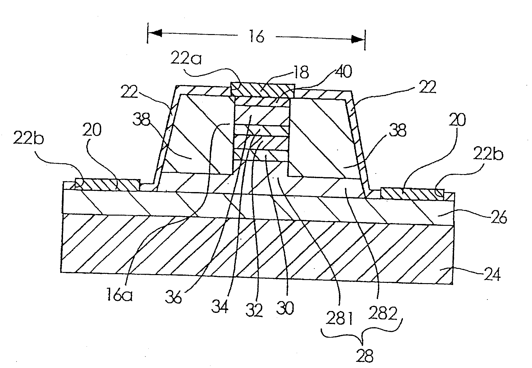
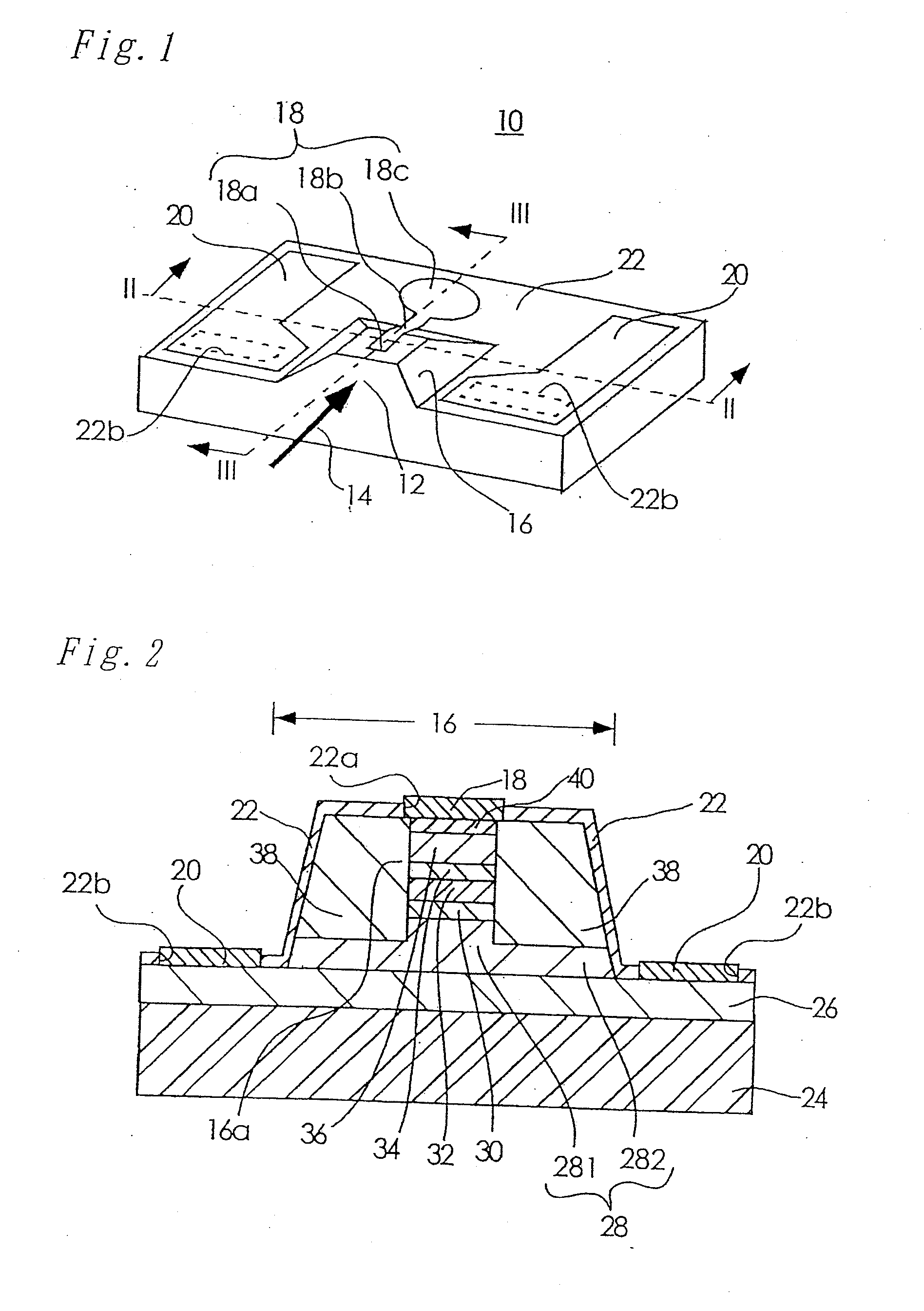
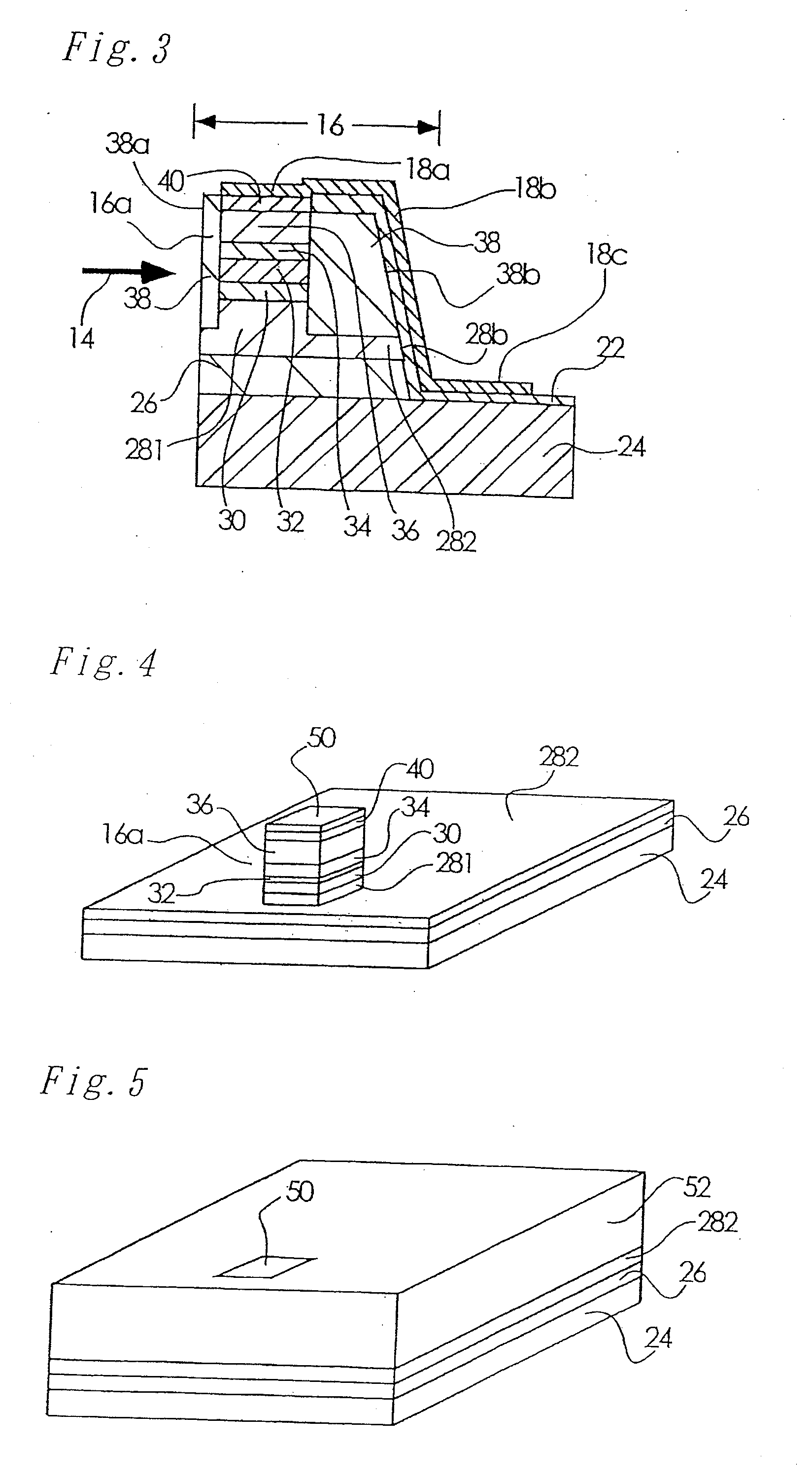
[0035]FIG. 1 is a perspective view of a semiconductor photoreceptor device according to a first embodiment of the present invention. FIG. 2 is a cross-sectional view of the semiconductor photoreceptor device shown in FIG. 1 taken along line II-II, while FIG. 3 is a cross-sectional view of the same semiconductor photoreceptor device taken along line III-III. It should be noted that like numerals will be used to denote the same or corresponding components.

[0036]Referring to FIG. 1, a light receiving portion 12 in the front of this buried waveguide type PIN-PD 10 receives signal light 14 indicated by the arrow. A waveguide mesa 16 is formed such that it projects from the top surface of the PIN-PD 10. The waveguide mesa 16 includes a waveguide 16a to which the signal light is introduced through the light receiving portion 12, as shown in FIGS. 2 and 3. A p-electrode 18 (acting as a second electrode) is disposed along the top surface of the waveguide mesa 16 such that the p-electrode 18 ...

second embodiment

[0092]FIG. 11 is a perspective view of a semiconductor photoreceptor device according to a second embodiment of the present invention. FIG. 12 is a cross-sectional view of the semiconductor photoreceptor device shown in FIG. 11 taken along line XII-XII, while FIG. 13 is a cross-sectional view of the same semiconductor photoreceptor device taken along line XIII-XIII.

[0093]Referring to FIG. 11, a light receiving portion 12 in the front of this buried waveguide type PIN-PD 60 receives signal light 14 indicated by the arrow. On the top side of the PIN-PD 60 are disposed a waveguide 16a and a blocking layer 38 surrounding the waveguide 16a, as shown in FIGS. 12 and 13. The waveguide 16a receives the signal light through the light receiving portion 12. On both sides of the waveguide 16a are formed openings 62 that go through the blocking layer 38 and an n-cladding layer 28 to the surface of an n-contact layer 26, thus forming a waveguide mesa 16 which includes the waveguide 16a.

[0094]Eac...


PUM


Abstract

A semiconductor light detecting device includes an n-contact layer selectively disposed on an Fe—InP substrate. An optical waveguide layer is disposed on the n-contact layer and includes an n-cladding layer, a light absorption layer, and a p-cladding layer, laminated on one another over the n-contact layer, in that order. An Fe—InP current blocking layer is disposed on the n-cladding layer such that sides of the optical waveguide layer are buried in the Fe—InP current blocking layer. A p-electrode includes a contact electrode electrically connected to the p-cladding layer of the optical waveguide layer, a lead-out electrode portion extending on a side wall of the current blocking layer from the contact electrode and extending on the Fe—InP substrate, and an electrode pad disposed on a surface of the Fe—InP substrates with an SiN film between the electrode pad and the surface of the Fe—InP substrate and connected to the lead-out electrode portion.

Description

BACKGROUND OF THE INVENTION[0001]1. Field of the Invention[0002]The present invention relates to a semiconductor photoreceptor device and a manufacturing method therefor, and more particularly to a semiconductor photoreceptor device used for optical communications systems, etc. and a manufacturing method therefor.[0003]2. Background Art[0004]The capacity of communications systems has been increased to satisfy the dramatically increasing demand for communications. Accordingly, there has been a need for higher-speed, higher-efficiency yet lower-cost and smaller optical communications devices.[0005]In transmission systems for optical communications, efforts are being made to develop and improve high-speed optical communications devices to accommodate 40-GHz band signal light.[0006]One factor in determining the response speed of semiconductor photoreceptor devices such as PIN photodiodes and avalanche photodiodes is their CR time constant. (The term “photodiode” is hereinafter abbreviat...

Claims


Application Information

Patent Timeline
Patent Type & Authority Applications(United States)
IPC IPC(8): H01L31/0232
CPCG02B6/122H01L31/105H01L31/0232H01L31/02327
Inventor NAKAJI, MASAHARUISHIMURA, EITARO
Owner MITSUBISHI ELECTRIC CORP
Why Eureka
Try Eureka