Solid-state imaging device and manufacturing method thereof

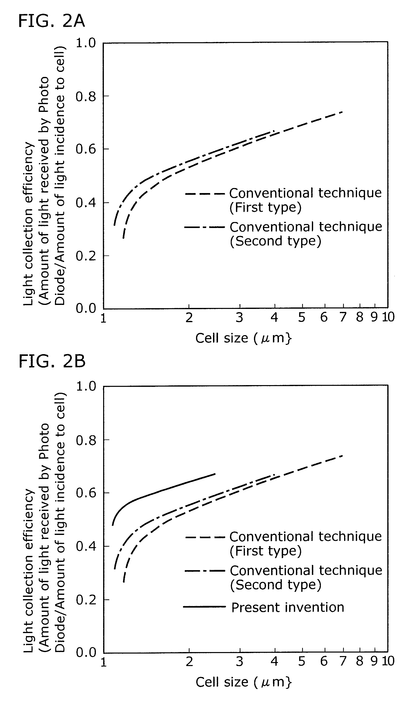
a solid-state imaging and manufacturing method technology, applied in the direction of solid-state devices, color television, television systems, etc., can solve the problems of reducing the light collection efficiency to 50% or below, the impracticality of solid-state imaging devices, and the more practicability of the first-type conventional technique, etc., to achieve excellent color separation characteristics, eliminate loss, and highlight collection efficiency

Inactive Publication Date: 2009-10-08
PANASONIC CORP
View PDF13 Cites 16 Cited by
  • Summary
  • Abstract
  • Description
  • Claims
  • Application Information

AI Technical Summary

Benefits of technology

[0022]The light absorbing particles, provided in at least one of the plural types of optical waveguide regions, include organic molecules. This structure can provide a waveguide having excellent color separation characteristics thanks to the characteristics of organic molecules showing absorption transmission characteristics only for a particular wavelength of visible light.
[0023]The solid-state imaging device further includes read circuits each of which reads out a signal charge from one of the plural photoelectric conversion elements, wherein an insulating region is formed: between the plural optical waveguide regions and the plural of photoelectric conversion elements; and between said plural optical waveguide regions and said read circuit. This structure can ensure to prevent the waveguide regions including the metal particles from es

Problems solved by technology

Minimizing the cell size to 1.5 μm or smaller significantly lowers the light collection efficiency to 50% or below and makes the solid-state imaging devices impractical even with the second-type conventional technique.
It is more impractical with the first-type conventional technique.
One of the causes of the problem is that a l

Method used


Image

  • Solid-state imaging device and manufacturing method thereof
  • Solid-state imaging device and manufacturing method thereof
  • Solid-state imaging device and manufacturing method thereof

Examples


first embodiment

[0056]A solid-state imaging device in a first embodiment of the present invention and a manufacturing method thereof shall be described with reference to FIGS. 4A through 10.

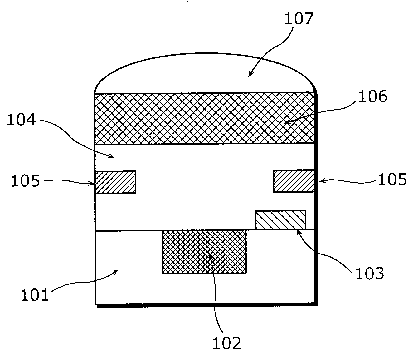
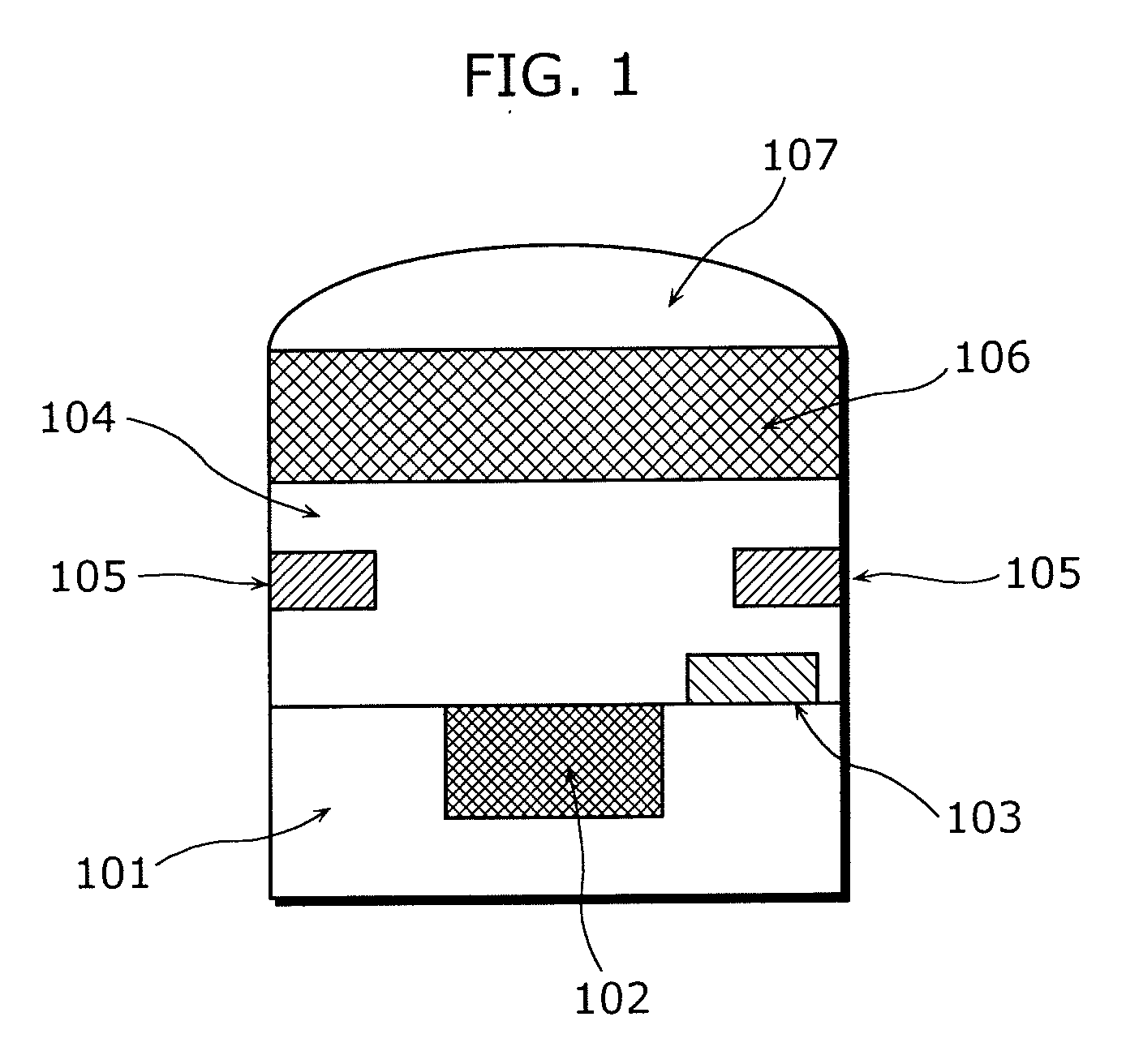
[0057]FIG. 4A illustrates cross-sectional views of three pixel units in red, green, and blue in the solid-state imaging device of the embodiment. FIG. 4A shows that a photodiode 102, a read-out circuit 103 reading out an output signal from the photodiode 102, and metal lines 105 and 105′ are formed in each of pixel units on a surface of an Si substrate 101. The metal lines 105 and 105′ are provided in an interlayer insulating film 104 chiefly made of SiO2. Each of the pixel units is 1.5 μm in size. In a portion of the interlayer insulating film 104 on each of photodiodes 104, an optical waveguide 401, an optical waveguide 402, and an optical waveguide 403 are formed. The optical waveguide 401 transmits a red wavelength region light, and absorbs the lights of the other wavelength regions. The optical waveguide 40...

second embodiment

[0071]A solid-state imaging device in a second embodiment of the present invention and a manufacturing method thereof shall be described with reference to FIG. 11 through FIG. 16.

[0072]FIG. 11 illustrates cross-sectional views of three pixel units in red, green, and blue in the solid-state imaging device of the embodiment. FIG. 11 shows that the photodiode 102, an output signal read-out circuit 103 thereof, and metal lines 105 and 105′ are formed in each of pixel units on a surface of an Si substrate 101. The metal lines 105 and 105′ are provided in an interlayer insulating film 104 chiefly made of SiO2. Each of the pixels is 1.5 μm in size. In a portion of the interlayer insulating film 104 on each of photodiodes 102, an optical waveguide 1101, an optical waveguide 1102, and an optical waveguide 1103 are formed. The optical waveguide 1101 transmits a red wavelength region light and absorbs the lights of the other wavelength regions. The optical waveguide 1102 transmits a green wave...

third embodiment

[0084]A solid-state imaging device in a third embodiment of the present invention and a manufacturing method thereof shall be described with reference to FIGS. 17 through FIG. 23.

[0085]FIG. 17 illustrates cross-sectional views of three pixel units in red, green, and blue in the solid-state imaging device of the embodiment. FIG. 17 shows that the photodiode 102, the output signal read-out circuit 103 thereof, and the metal lines 105 and 105′ are formed in each of pixel units on a surface of the Si substrate 101. The metal lines 105 and 105′ are provided in the interlayer insulating film 104 chiefly made of SiO2. Each of the pixels is 1.5 μm in size. In a portion of the interlayer insulating film 104 on each of photodiodes 102, an optical waveguide 1701, an optical waveguide 1702, and an optical waveguide 1703 are formed. The optical waveguide 1701 transmits a red wavelength region light and absorbs the lights of the other wavelength regions. The optical waveguide 1702 transmits a gre...


PUM


Abstract

A solid-state imaging device in the present invention includes plural photoelectric conversion elements, plural wiring layers, and plural optical waveguide regions each corresponding to and arranged over one of the plural photoelectric conversion elements. A top end of each of the plural optical waveguide regions is higher than a top end of at least one of the plural wiring layers. A bottom end of each of the plural optical waveguide regions is lower than a bottom end of at least one of the plural wiring layers. The plural optical waveguide regions include plural types of optical waveguide regions each having different light absorbing characteristics.

Description

BACKGROUND OF THE INVENTION[0001](1) Field of the Invention[0002]The present invention relates to a solid-state imaging device which is capable of optical waveguiding and color separating, and a manufacturing method thereof.[0003](2) Description of the Related Art[0004]Solid-state imaging devices including MOS sensors and charge coupled devices (CCD) are embedded in digital cameras and cellular phones. Increasing demands for higher definition imaging and further downsizing of the digital cameras and cellular phones lead to miniaturization of the devices, and the pixels (cells) therein. FIG. 1 is a cross-sectional schematic view of a pixel unit of a conventional MOS sensor in a first type. A photoelectric conversion element (photodiode) 102 and a read-out circuit 103, adjacent to the photodiode 102, reading out an output electrical charge provided from the photodiode 102 are formed on the surface of an Si substrate 101. A metal line 105 is formed in an interlayer insulating film 104....

Claims


Application Information

Patent Timeline
IPC IPC(8): H01L31/0232H01L21/00H01L27/14H04N5/335H04N5/369H04N5/372H04N5/374
CPCH01L27/14621H01L27/14629H01L27/14685
Inventor HIROSE, YUTAKATANAKA, KEISUKESAITOU, SHIGERUUEDA, DAISUKE
Owner PANASONIC CORP
Why Eureka
Try Eureka