Multi-chip stack package

Active Publication Date: 2009-10-08
NAN YA TECH
View PDF18 Cites 75 Cited by
  • Summary
  • Abstract
  • Description
  • Claims
  • Application Information

AI Technical Summary

Benefits of technology

[0010]The present invention provides a multi-chip stack package which h

Problems solved by technology

Hence, the problem of signal delay occurs during the operation of the multi-chip stack package 100.
However, the contacts may not be arranged according to the designer's requirement.
However, the width (between 5-10 micrometers) of the circuits of the redistribution layer is becoming smaller and smaller, and the material thereof generally comprises gold, which is expensive and has bad electrical conductivity.
Thus, the conventio

Method used


Image

  • Multi-chip stack package
  • Multi-chip stack package
  • Multi-chip stack package

Examples


Example

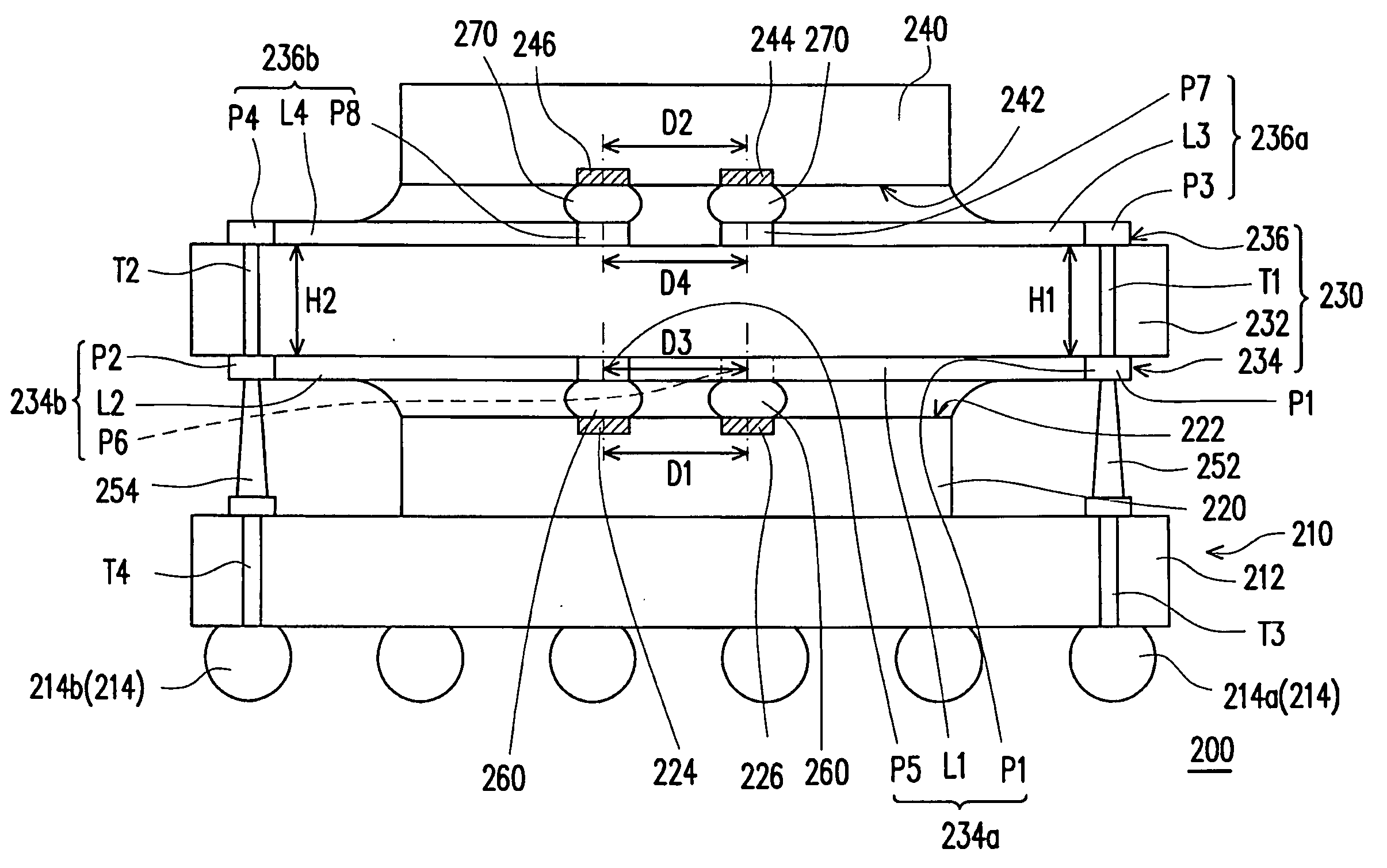
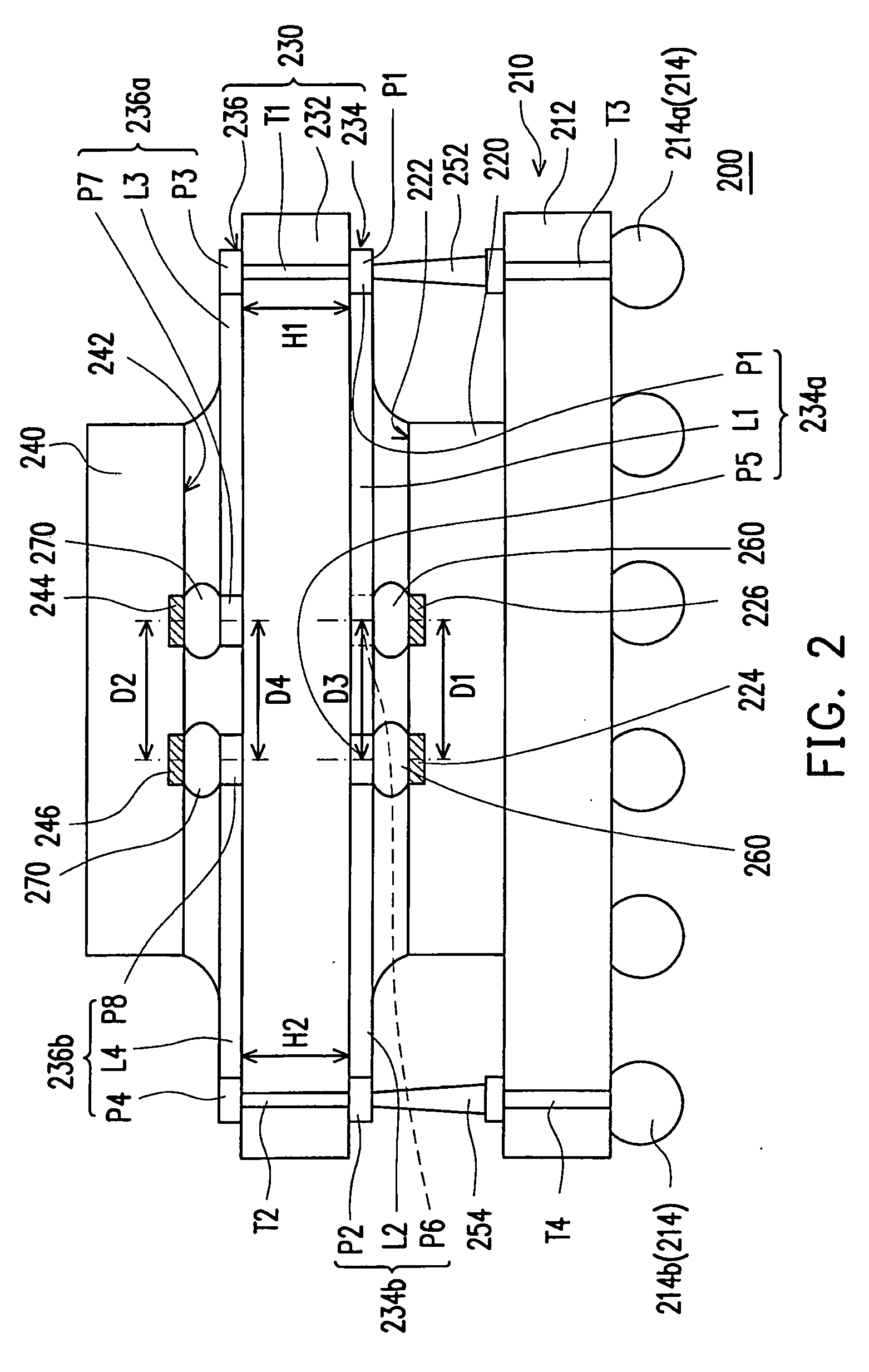
[0030]FIG. 2 is a schematic cross-sectional view of a multi-chip stack package according to an embodiment of the present invention. FIG. 3 is an analytic schematic view of a first chip, a second wiring substrate, and a second chip in FIG. 2.

[0031]Referring to FIG. 2 and FIG. 3, a multi-chip stack package 200 comprises a first wiring substrate 210 such as a print circuit board, a first chip 220 such as a memory chip, a second wiring substrate 230, and a second chip 240 such as a memory chip. The first chip 220 is disposed on a front side (not shown) of the first wiring substrate 210 and has a first active surface 222 which is directed to a first direction away from the first wiring substrate 210 without directly contacting the front side of the first wiring substrate 210.

[0032]The second wiring substrate 230 is disposed on the first active surface 222 of the first chip 220 and comprises a dielectric layer 232, a first wiring layer 234, and a second wiring layer 236, wherein the first...


PUM


Abstract

A multi-chip stack package comprising a first wiring substrate, a first chip, a second wiring substrate, and a second chip is provided. The first wiring substrate is with a front side and a rear side. The first chip is disposed on the front side of the first wiring substrate and electrically connected to the first wiring substrate and the first chip has a first active surface. The second wiring substrate is disposed on the first active surface of the first chip and electrically connected to the first wiring substrate. The second chip is disposed on the second wiring substrate and electrically connected to the second wiring layer. The second active surface of the second chip faces the first active surface of the first chip.

Description

CROSS-REFERENCE TO RELATED APPLICATION[0001]This application claims the priority benefit of Taiwan application serial no. 97112491, filed on Apr. 7, 2008. The entirety of the above-mentioned patent application is hereby incorporated by reference herein and made a part of this specification.BACKGROUND OF THE INVENTION[0002]1. Field of the Invention[0003]The present invention relates to a multi-chip stack package assembly, and particularly relates to a multi-chip stack package which has better signal transmission efficiency and requires lower fabrication costs.[0004]2. Description of Related Art[0005]Along with the ongoing development of electronic technology, new generations of electronic products with more complex and user-friendly functions are coming forth to replace old products. In addition, new electronic products are designed to be lighter, thinner, shorter, and smaller. Accordingly, various high-density semiconductor packages are developed in semiconductor package technology,...

Claims


Application Information

Patent Timeline
IPC IPC(8): H01L23/52
CPCH01L21/563H01L23/49838H01L23/5385H01L25/0657H01L2224/16225H01L2224/48091H01L24/48H01L2225/06517H01L2225/0652H01L2225/06527H01L2225/06572H01L2224/48227H01L2924/00014H01L2224/023H01L2224/05571H01L2224/05573H01L2924/15184H01L2224/05599H01L2224/45099H01L2224/45015H01L2924/207H01L2924/0001
Inventor CHEN, JEN-CHUNYANG, WU-DER
Owner NAN YA TECH
Why Eureka
Try Eureka