Device for protecting an integrated circuit against a laser attack

a technology for integrated circuits and laser attacks, applied in pulse generators, pulse techniques, electric pulse generator circuits, etc., can solve the problems of integrated circuit manufacturing costs, only enabling the detection of laser attacks, and the protection device cannot protect the integrated circui

Inactive Publication Date: 2009-10-08
STMICROELECTRONICS (ROUSSET) SAS
View PDF4 Cites 32 Cited by
  • Summary
  • Abstract
  • Description
  • Claims
  • Application Information

AI Technical Summary

Benefits of technology

[0009]At least one embodiment of the present invention aims at a device for protecting an integrated circuit against laser attacks, enabling

Problems solved by technology

However, such a protection device only enables detection a laser attack if the laser beam directly reaches one of the sensors of the protection device.
This ne

Method used


Image

  • Device for protecting an integrated circuit against a laser attack
  • Device for protecting an integrated circuit against a laser attack
  • Device for protecting an integrated circuit against a laser attack

Examples


Embodiment Construction

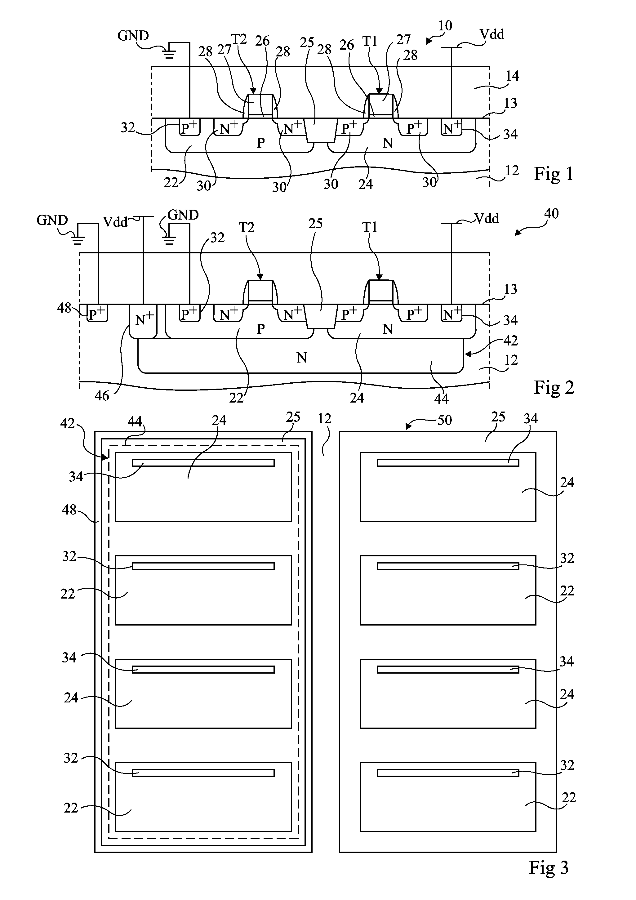
[0028]For clarity, the same elements have been designated with the same reference numerals in the different drawings and, further, as usual in the representation of integrated circuits, the various drawings are not to scale. In the following description, the portions of the integrated circuit substrate at the level of which electronic components such as transistors, diodes, etc. are formed are called active areas of the integrated circuit. More specifically, in the context of the present invention, integrated circuits for which the active areas extend into the substrate from a surface of the substrate only down to part of the substrate depth are considered.

[0029]FIG. 1 is a simplified cross-section view of an example of a conventional integrated circuit. Integrated circuit 10 comprises a substrate 12 of a semiconductor material. It is, for example, an undoped or P-type doped single-crystal silicon substrate 12. Substrate 12 comprises a surface 13 covered with a stack of insulating l...


PUM


Abstract

An integrated circuit including a substrate of a semiconductor material having first and second opposite surfaces and including active areas leveling the first surface. The integrated circuit includes a device of protection against laser attacks, the protection device includes at least one first doped region extending between at least part of the active areas and the second surface, a device for biasing the first region, and a device for detecting an increase in the current provided by the biasing device.

Description

CROSS REFERENCE TO RELATED APPLICATIONS[0001]This application claims the priority benefit of French patent application number 08 / 52215, filed on Apr. 3, 2008, entitled “DEVICE FOR PROTECTING AN INTEGRATED CIRCUIT AGAINST A LASER ATTACK,” which is hereby incorporated by reference to the maximum extent allowable by law.BACKGROUND OF THE INVENTION [0002]1. Field of the Invention[0003]The present invention relates to devices for protecting an integrated circuit against external attacks.[0004]2. Discussion of the Related Art[0005]It may be desirable to protect an integrated circuit against external attacks aiming, for example, at disturbing or even hindering the normal operation of the integrated circuit. An example of attack comprises scanning the front surface or the rear surface of the integrated circuit with a laser, especially a pulse laser. Such a method can enable to modify data stored in memories of the integrated circuit or to modify the logic states or the durations of signals ...

Claims


Application Information

Patent Timeline
IPC IPC(8): H03K19/00H01L21/265H01L31/00
CPCH01L23/576H01L2924/0002H01L2924/00
Inventor LISART, MATHIEUPOUGET, VINCENT
Owner STMICROELECTRONICS (ROUSSET) SAS
Why Eureka
Try Eureka