Semiconductor Device

a memory device and semiconductor technology, applied in the direction of information storage, static storage, digital storage, etc., can solve the problems of data not being written in the memory element, data cannot be written, and data cannot be written

Active Publication Date: 2009-10-08
SEMICON ENERGY LAB CO LTD
View PDF16 Cites 42 Cited by
  • Summary
  • Abstract
  • Description
  • Claims
  • Application Information

AI Technical Summary

Benefits of technology

[0017]According to another embodiment of the present invention, dielectric breakdown of a transistor can be suppressed and data can be written correctly in a memory element.

Problems solved by technology

Thus, when the potential of the bit line is applied to the memory element through the select transistor, dielectric breakdown occurs in the select transistor, and there is a possibility that data cannot be written in the memory element.
Particularly when the voltage (also referred to as the writing voltage) necessary for wiring data in a memory element is higher than the level of the withstand voltage of the select transistor, in writing operation, dielectric breakdown occurs in the select transistor when voltage necessary for wiring data in the memory element (also referred to as the writing voltage) is applied, so that there is a possibility that data cannot be written.

Method used


Image

  • Semiconductor Device
  • Semiconductor Device
  • Semiconductor Device

Examples


embodiment 1

[0034]In this embodiment, one embodiment of a semiconductor memory device of the present invention is described.

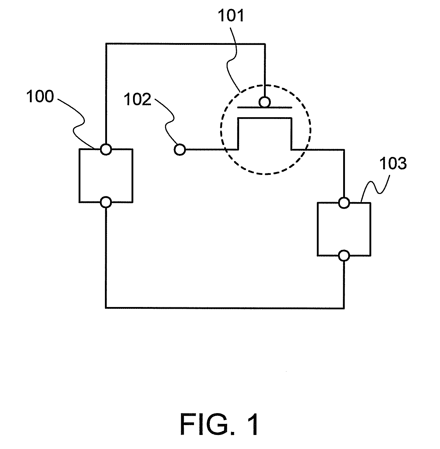
[0035]First, a structure of a semiconductor memory device in this embodiment is described with reference to FIG. 1. FIG. 1 is a circuit diagram which illustrates the structure of the semiconductor memory device in this embodiment.

[0036]As illustrated in FIG. 1, the semiconductor memory device in this embodiment includes a potential control circuit 100, a transistor 101, a potential supply terminal 102, and a memory element 103.

[0037]The potential control circuit 100 includes an input terminal, a first output terminal, and a second output terminal; however, the input terminal is not illustrated in FIG. 1, and only the first output terminal and the second output terminal are illustrated. In addition, the transistor 101 includes a gate terminal, a source terminal, and a drain terminal. The gate terminal is electrically connected to the first output terminal of the potential c...

embodiment 2

[0053]In this embodiment, one embodiment of a specific structure of the semiconductor device described in Embodiment 1 is described.

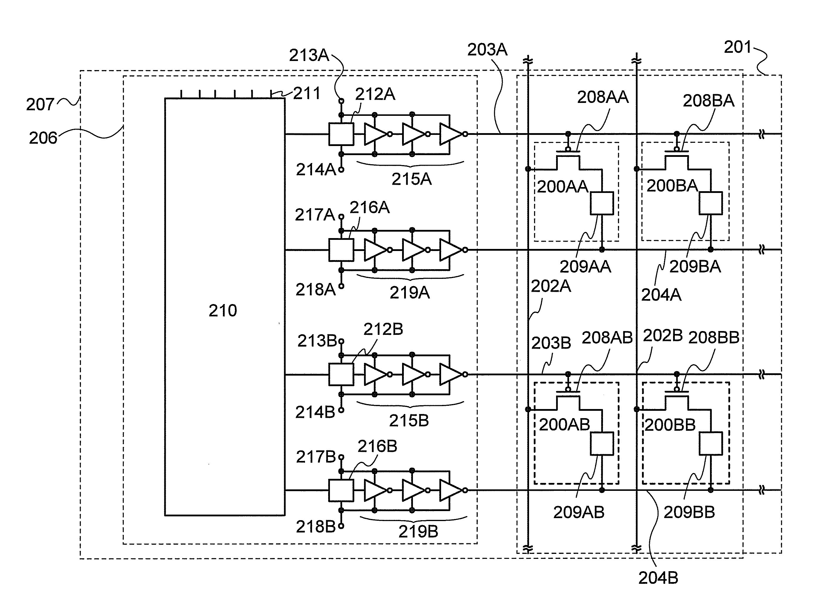
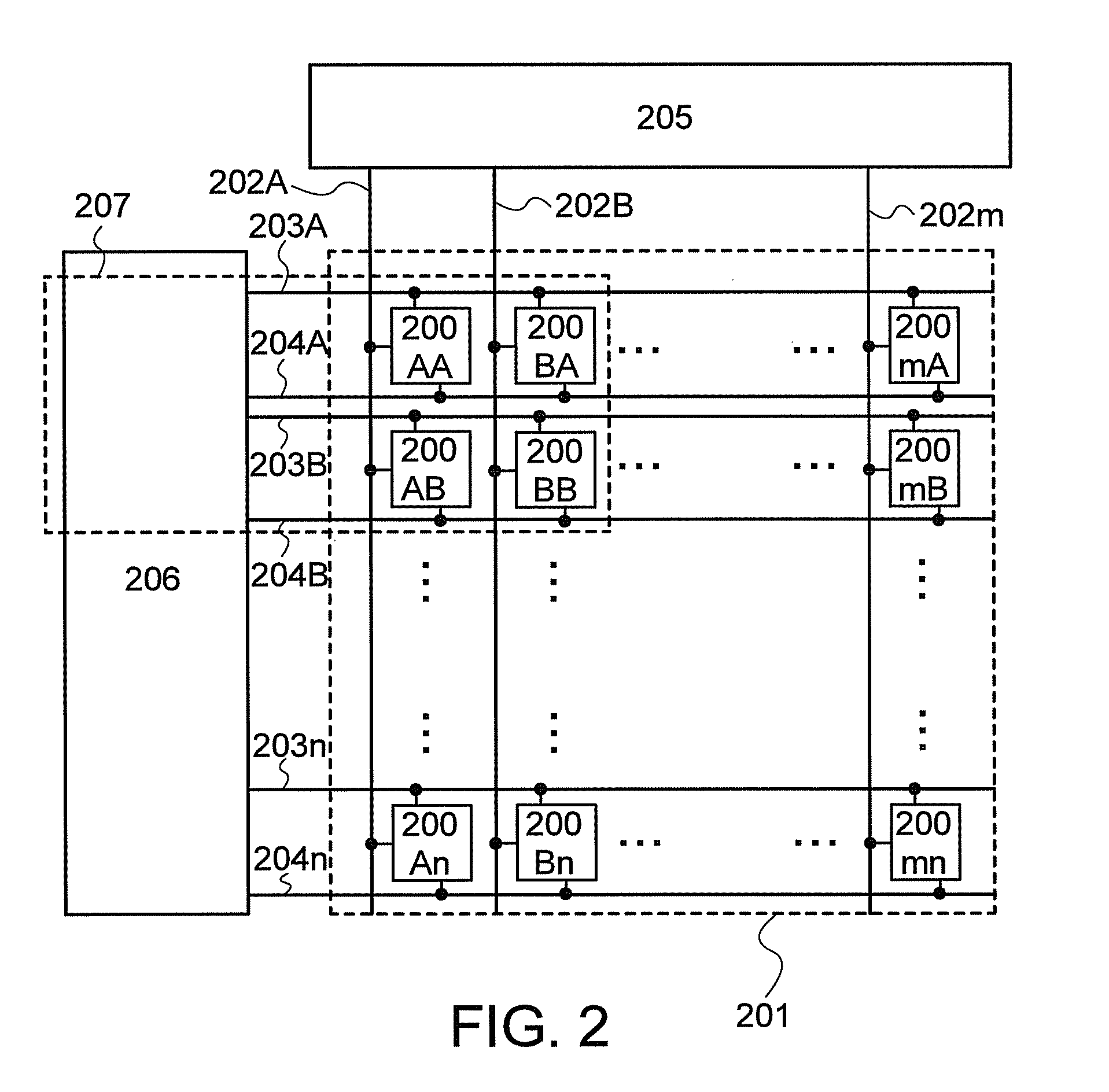
[0054]First, a structure of a semiconductor memory device in this embodiment is described with reference to FIG. 2. FIG. 2 is a block diagram illustrating the structure of the semiconductor memory device in this embodiment.

[0055]As illustrated in FIG. 2, the semiconductor memory device in this embodiment includes the following: a memory circuit portion 201 including a plurality of memory circuits 200 of m rows and n columns in which a first row includes a plurality of memory circuits 200 from a memory circuit 200AA to a memory circuit 200mA and a first column includes a plurality of memory circuits 200 from the memory circuit 200AA to a memory circuit 200An with reference to the memory circuit 200AA; a plurality of bit lines 202 including bit lines 202A to 202m; a plurality of first word lines 203 including first word lines 203A to 203n; a plurality of ...

embodiment 3

[0115]In this embodiment, a semiconductor memory device (also referred to as an organic memory) in which a memory element using an organic compound is applied to a memory circuit as an example of a semiconductor memory device of the present invention is described.

[0116]A structure of an organic memory in this embodiment is described with reference to FIGS. 6A and 6B and FIG. 7. FIGS. 6A and 6B are top views illustrating a structure of a memory circuit of a semiconductor memory device in this embodiment. FIG. 7 is a cross-sectional view illustrating a structure of a memory circuit of a semiconductor memory device in this embodiment. Note that FIGS. 6A and 6B and FIG. 7 typically illustrate the semiconductor device for convenience, and all of or part of them is illustrated with use of the dimensions which are different from the actual dimension.

[0117]As illustrated in FIG. 6A, the memory circuit of the semiconductor memory device in this embodiment includes a semiconductor layer 300, ...


PUM


Abstract

A semiconductor device is provided, which includes a transistor, a memory element, a first control circuit and a second control circuit. A gate of the transistor is electrically connected to the first control circuit through a first word line, one of a source and a drain of the transistor is electrically connected to the second control circuit through a bit line, the other of the source and the drain of the transistor is electrically connected to a first terminal of the memory element, and a second terminal of the memory element is electrically connected to the first control circuit through a second word line.

Description

BACKGROUND OF THE INVENTION[0001]1. Field of the Invention[0002]The present invention relates to a semiconductor memory device. Further, the present invention relates to a semiconductor device including the semiconductor memory device.[0003]2. Description of the Related Art[0004]In recent years, most electronic devices such as computers can perform desired operations by using a variety of data. When the data is held in, for example, a memory device (also referred to as a memory) or the like, the data can be used temporarily or semipermanently. A memory device also includes an external memory device (an auxiliary memory device) such as a hard disk or a flexible disk in a broad sense. However, a memory device almost always refers to a semiconductor memory device such as a CPU (central processing unit). Two main types of memory devices are a volatile memory and a nonvolatile memory. A volatile memory refers to a memory device in which data is lost over time after the data is held. A no...

Claims


Application Information

Patent Timeline
Patent Type & Authority Applications(United States)
IPC IPC(8): G11C5/06G11C7/00
CPCG11C13/0004G11C13/0014G11C13/003G11C2213/79G11C2013/0071G11C2013/009G11C2213/76G11C13/0069
Inventor SAITO, TOSHIHIKO
Owner SEMICON ENERGY LAB CO LTD
Why Eureka
Try Eureka