Electronic circuit

a technology of electrical circuits and circuits, applied in the direction of oscillator generators, pulse automatic control, electrical apparatus, etc., can solve the problems of differential non-linearity, inability to understand differential non-linearity, and inability to produce out-of-band phase errors of sigma delta modulators, so as to reduce the q factor of the lc loop, and reduce the parasitic capacitance.

Active Publication Date: 2009-10-22
TELEFON AB LM ERICSSON (PUBL)
View PDF1 Cites 0 Cited by
  • Summary
  • Abstract
  • Description
  • Claims
  • Application Information

AI Technical Summary

Benefits of technology

[0014]A further embodiment provides an electric circuit, for use in a digital phase lock loop circuit, the electric current comprising: a first circuit element, being a phase detector or a charge pump; the first circuit element comprising at least one power supply point and at least one output; wherein parasitic capacitances exists between said current paths; and said current paths are arranged in order to minimise said parasitic capacitances.
[0015]Another embodiment further provides an electric circuit, for use in a digital phase lock loop circuit, the electric circuit including a first circuit element being a phase frequency detector or a charge pump, the first element being connected via conductive tracks to power supply rails, wherein, in operation, parasitic inductances are formed along said conductive tracks and parasitic capacitances are formed between said supply rails such that LC resonant loops are formed which include said first circuit element, the electric circuit further comprising resistors connected between the conductive tracks and the power supply rails such that the resistors are connected in series with said parasitic inductances, the resistors reducing the Q factor of the LC resonant loops, thereby to reduce the non-linearity at the output of the first circuit element.
[0016]Another embodiment further provides a method of reducing non-linearity in a digital phase lock loop phase frequency detector circuit, the circuit comprising a first circuit element, being a phase frequency detector or a charge pump, the method comprising: identifying LC current loops formed by parasitic inductances and capacitances and which include the first circuit element; placing resistors in series with the parasitic inductances in order to reduce the Q factor of the LC loops.
[0017]Another embodiment further provides a method of reducing non-linearity in a digital phase lock loop phase frequency detector circuit, the circuit comprising a first circuit element, being a phase frequency detector or a charge pump, the method comprising: identifying LC current loops formed by parasitic inductances and capacitances and which include the first circuit element; placing at least one capacitor in parallel with the first circuit element in order to reduce the current flowing in the parasitic inductances.

Problems solved by technology

Sigma delta modulators produce out-of-band phase errors.
This creates in-band noise and spurs.
Differential non-linearity is not particularly well understood and there has been little or no identification or study of the causes of differential non-linearity in the available technical literature.

Method used


Image

  • Electronic circuit
  • Electronic circuit
  • Electronic circuit

Examples


Embodiment Construction

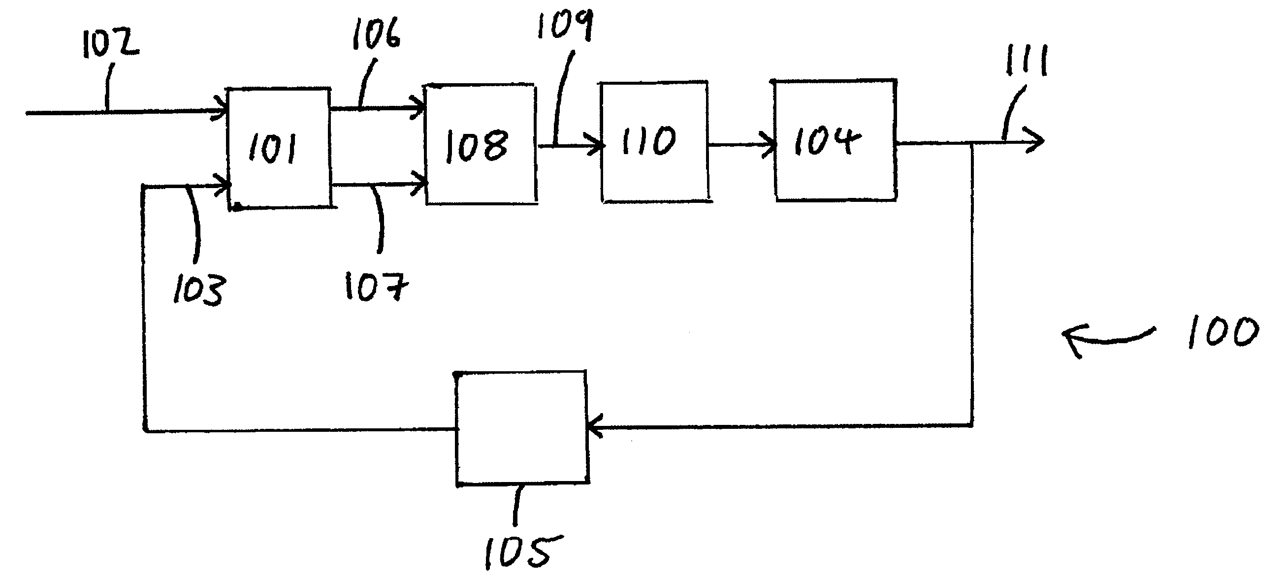
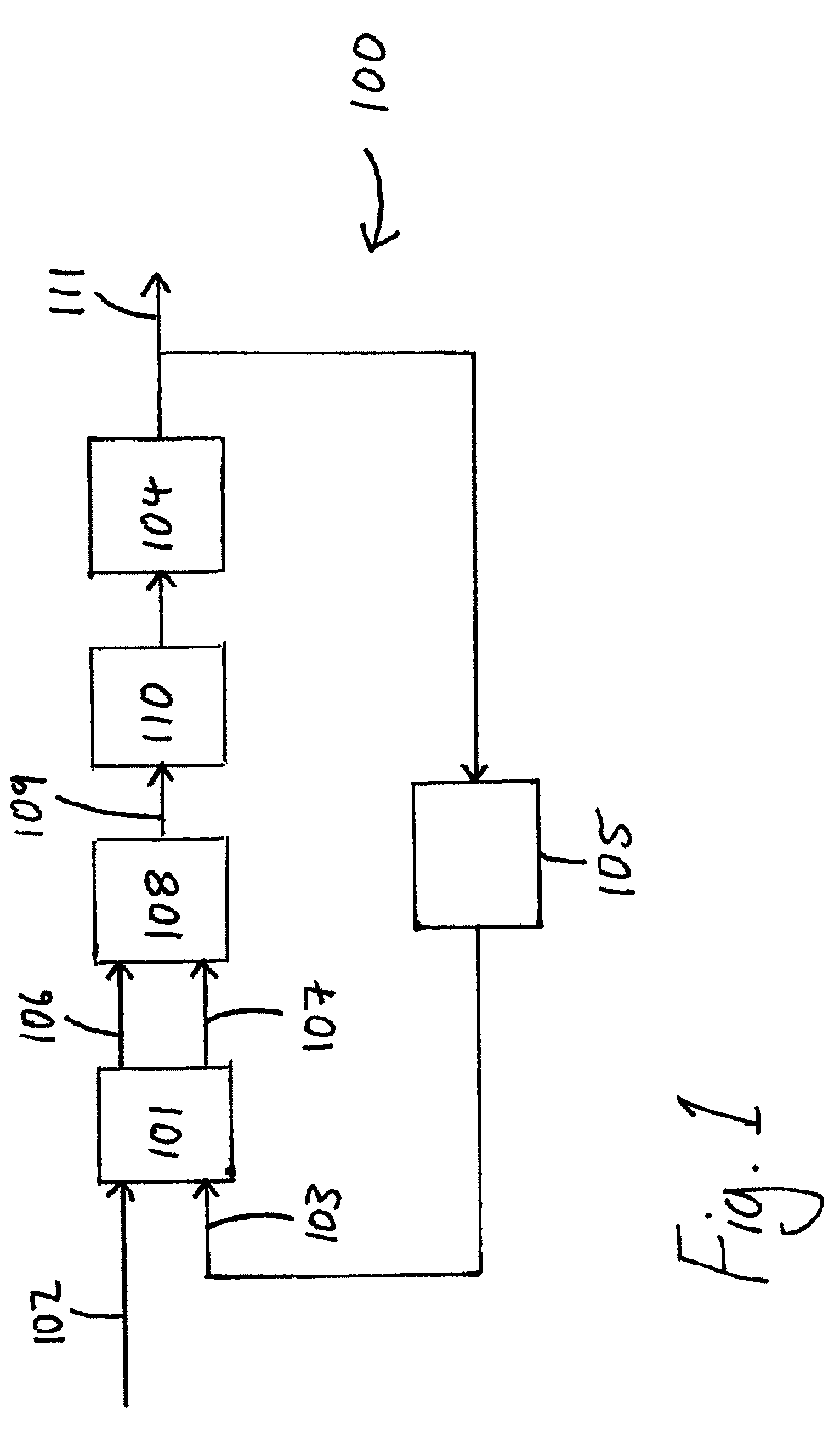
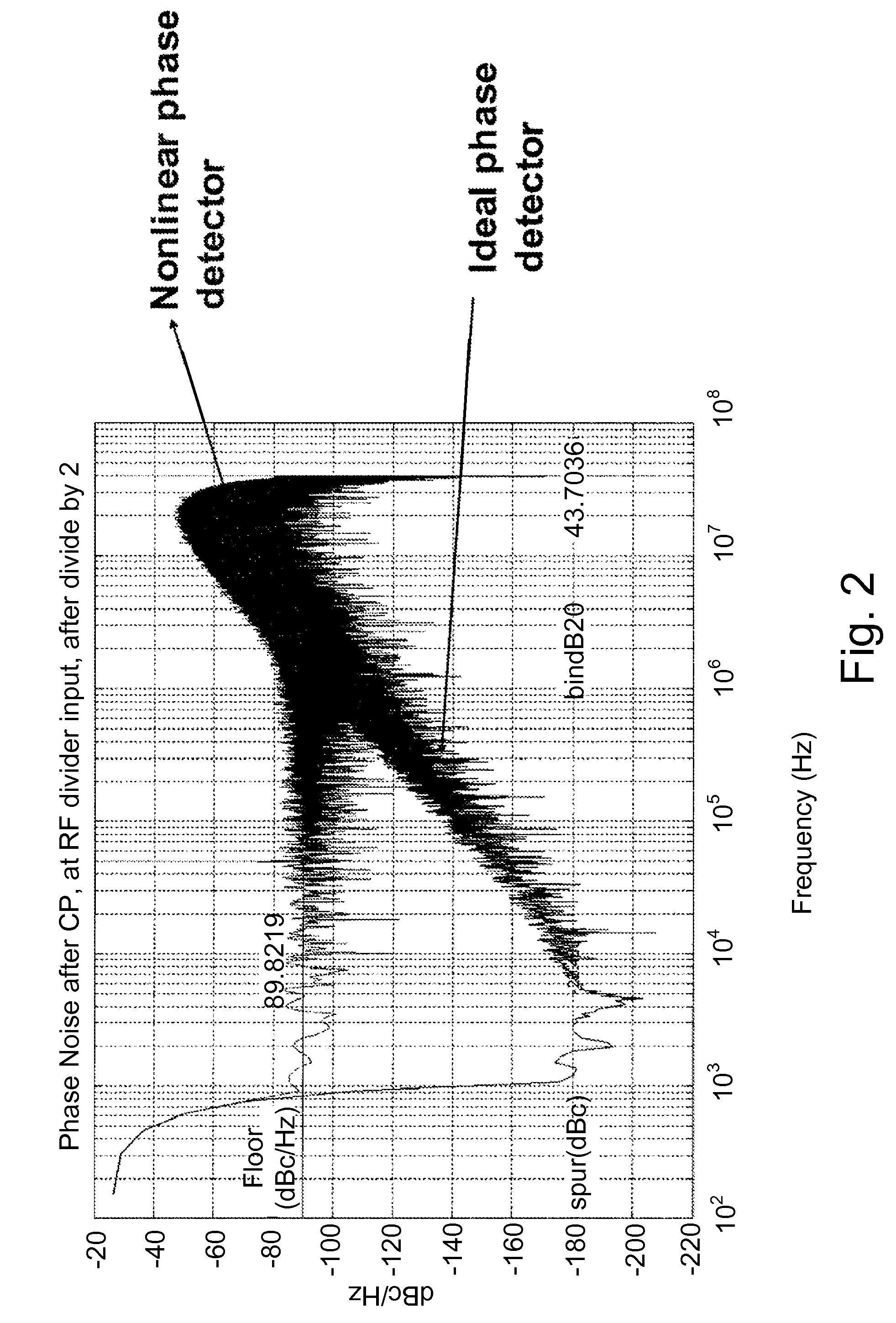
[0026]The Applicant has investigated the causes of differential non-linearity in phase frequency detectors and charge pump circuits. FIG. 5 shows a charge pump 200 which is connected to power rails VDD 201 and VSS 202. The charge pump 200 is connected to VDD 201 via routing 203. The charge pump 200 is connected to VSS 202 via routing 204. The charge pump 200 has a single output 205 which includes routing 206. Routing 203, 204 and 206 each produce parasitic inductances 207, 208 and 209 during the operation of the charge pump 200. These routings can be either inside a chip in which the circuit is formed or inside a board on which the chip is mounted. In addition to parasitic inductances 207, 208, 209, the circuit shown in FIG. 5 includes parasitic capacitances 210, 211 and 212. The parasitic capacitances exist between output routing 206, supply rail VDD 201 and supply rail VSS 202.

[0027]In use, when the charge pump circuit 200 receives an UP signal, the charge pump drives current betw...


PUM


Abstract

An electric circuit, for use in a phase lock loop circuit, the electric circuit comprising: a first circuit element, being a phase frequency detector or a charge pump; at least one LC resonant loop, the first circuit element forming part of the loop; and means arranged to reduce ringing in said at least one LC resonant loop.

Description

FIELD OF THE INVENTION[0001]The present invention relates to an electric circuit for use in a phase lock loop circuit. In particular, the present invention relates to the design of phase frequency detectors and charge pumps, for use in such circuits.BACKGROUND AND PRIOR ART[0002]FIG. 1 shows a conventional fractional-n digital phase lock loop (PLL) circuit 100. The circuit includes a phase frequency detector (PFD) 101. The PFD 101 has two inputs. A first input 102 carries a reference signal. The reference signal is typically obtained from an incoming radio signal. A second input 103 originates from voltage controlled oscillator (VCO) 104. The output of the voltage controlled oscillator 104 is passed through divide by n counter 105. The output of the divide by n counter 105 is connected to the second input 103 of the PFD 101. The voltage control oscillator 104 and the divide by n counter 105 are set such that the signal arriving at the second input 103 is approximately the same frequ...

Claims


Application Information

Patent Timeline
Patent Type & Authority Applications(United States)
IPC IPC(8): H03L7/06
CPCH03L7/093H03L7/0895
Inventor CHOKKALINGAM, RAMESHCONTA, MATTEO
Owner TELEFON AB LM ERICSSON (PUBL)
Why Eureka
Try Eureka