Semiconductor laser device and method of manufacturing the same

a semiconductor laser and laser technology, applied in semiconductor lasers, laser details, nanooptics, etc., can solve the problems of ridge portion and damage to /i>(waveguides), and achieve the effects of suppressing the damage of the waveguide, and reducing the size of the semiconductor laser devi

Inactive Publication Date: 2009-10-22
SANYO ELECTRIC CO LTD
View PDF11 Cites 54 Cited by
  • Summary
  • Abstract
  • Description
  • Claims
  • Application Information

AI Technical Summary

Benefits of technology

[0008]The present invention has been proposed in order to solve the aforementioned problem, and an object of the present invention is to provide a semiconductor laser device capable of suppressing damage of a waveguide and a method of manufacturing the same.

Problems solved by technology

Therefore, there is such a problem that the ridge portion 102a (waveguide) may be damaged in bonding of the metal wire 108 to deteriorate laser characteristics.

Method used


Image

  • Semiconductor laser device and method of manufacturing the same
  • Semiconductor laser device and method of manufacturing the same
  • Semiconductor laser device and method of manufacturing the same

Examples


first embodiment

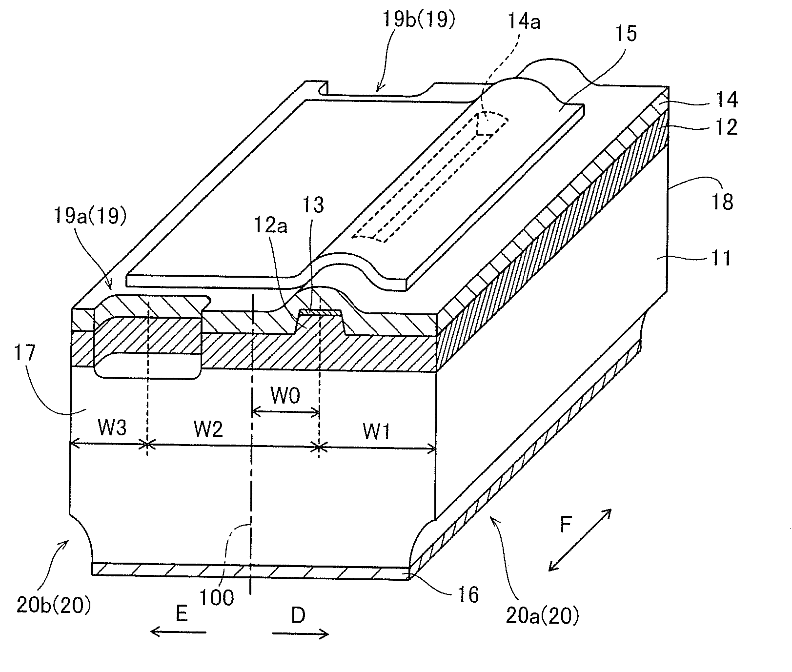
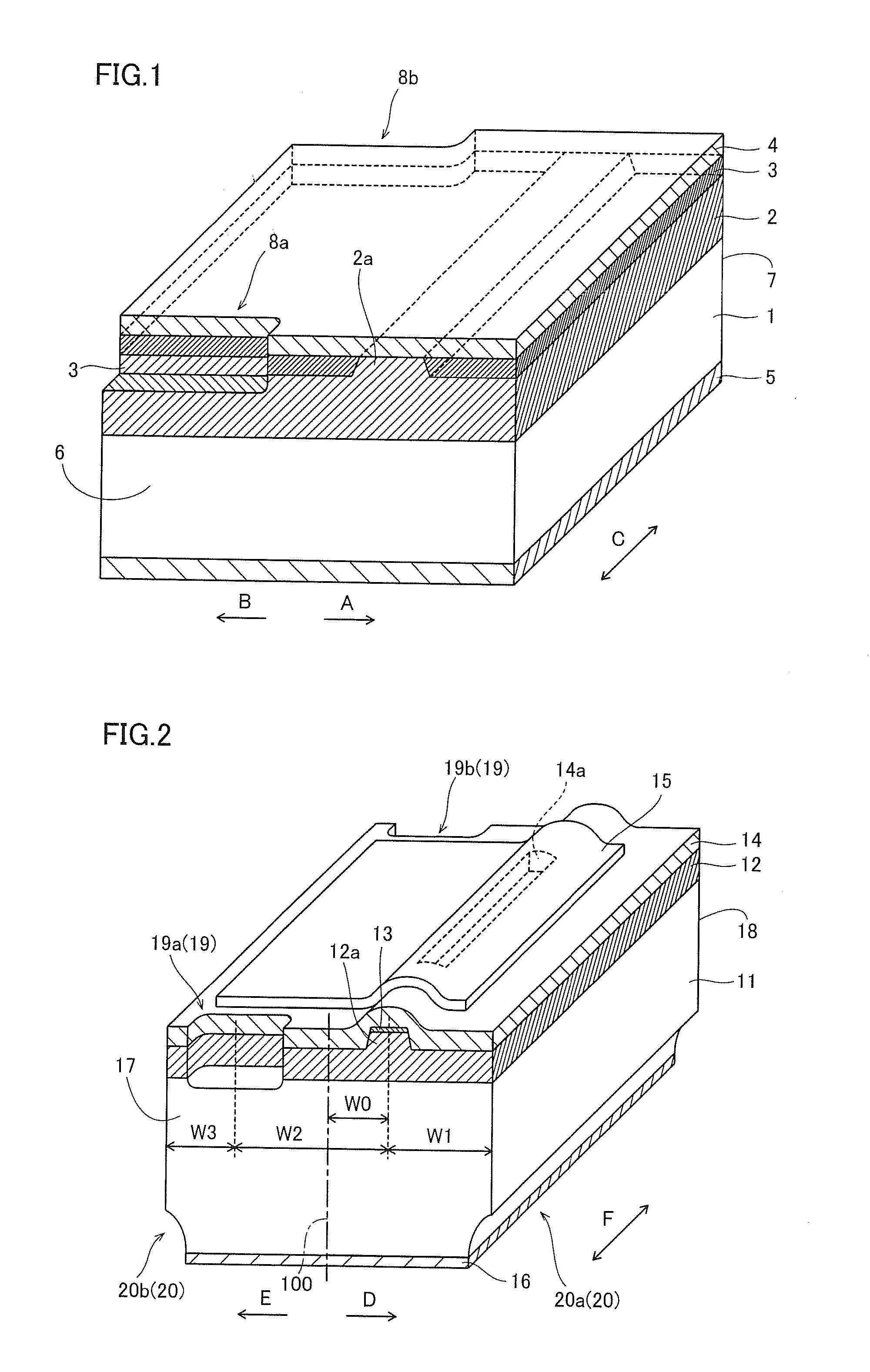
[0070]The structure of a GaN-based semiconductor laser chip according to a first embodiment is described with reference to FIGS. 2 and 3. In the first embodiment, the GaN-based semiconductor laser chip is described as an example of the semiconductor laser device according to the present invention. The GaN-based semiconductor laser chip according to the first embodiment is a 400 nm-band semiconductor laser chip (violet laser diode).

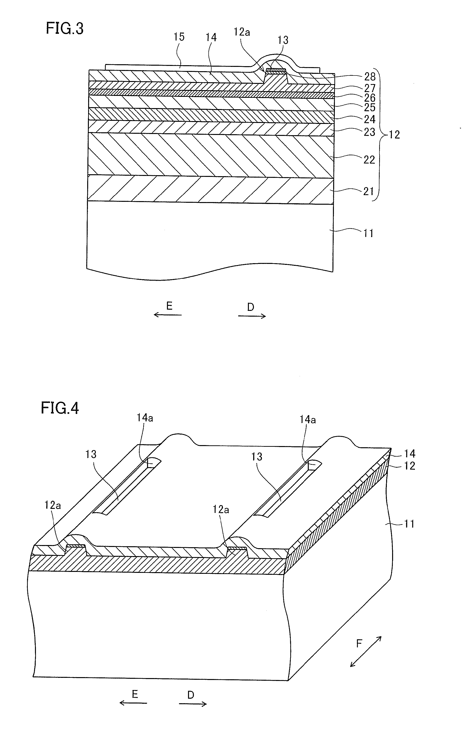
[0071]In the GaN-based semiconductor laser chip according to the first embodiment, a semiconductor layer 12 including an active layer 24 (see FIG. 3) described later and having a p-n junction is formed on an n-type GaN substrate 11, as shown in FIG. 2. This semiconductor layer 12 includes a ridge portion 12a constituting a waveguide extending in a direction F in a striped (slender) manner. The n-type GaN substrate 11 is an example of the “substrate” in the present invention. This GaN-based semiconductor laser chip is so formed that the length (width) along...

first modification

of First Embodiment

[0106]In this GaN-based semiconductor laser chip according to a first modification of the first embodiment, cleavage introduction steps 29a and 29b (second cleavage introduction recess portions 29) are formed also from a lower surface side (side of an n-type GaN substrate 11) in addition to cleavage introduction steps 19a and 19b formed from an upper surface side (side of a semiconductor layer 12) of the GaN-based semiconductor laser chip as shown in FIG. 10, dissimilarly to the aforementioned first embodiment. The cleavage introduction steps 29a and 29b are examples of the “third step” in the present invention. In particular, these cleavage introduction steps 29a and 29b are formed on the overall regions of cleavage planes 17 and 18 along a direction (along arrow D (along arrow E)) orthogonal to a ridge portion 12a (waveguide) respectively. According to this structure, a wafer can be more easily cleaved in the form of a bar in a manufacturing process (singulation...

second modification

of First Embodiment

[0107]In this GaN-based semiconductor laser chip according to a second modification of the first embodiment, cleavage introduction steps 29c and 29d (second cleavage introduction recess portions 29) are formed only on a partial region substantially opposite to cleavage introduction steps 19a and 19b and not formed on a region opposed to a ridge portion 12a (waveguide) as shown in FIG. 11, dissimilarly to the first modification of the aforementioned first embodiment. The cleavage introduction steps 29c and 29d are examples of the “third step” in the present invention. According to this structure, an impact following scribing can be inhibited from influencing the ridge portion 12a (waveguide) in a case of providing the cleavage introduction recess portions 29 with a diamond point in a state thinly forming an n-type GaN substrate 11, for example, in addition to effects similar to those of the first modification of the aforementioned first embodiment. According to the...


PUM


Abstract

A semiconductor laser device capable of suppressing damage of a waveguide is obtained. This GaN-based semiconductor laser chip (semiconductor laser device) includes an n-type GaN substrate of a nitride-based semiconductor and a semiconductor layer of a nitride-based semiconductor formed on the n-type GaN substrate and provided with a ridge portion constituting a waveguide extending in a direction F. The ridge portion (waveguide) is formed on a region approaching a first side from the center of the semiconductor layer. On a region opposite to the first side of the ridge portion (waveguide), a cleavage introduction step is formed from the side of the semiconductor layer, to extend in a direction intersecting with the extensional direction F of the ridge portion (waveguide).

Description

TECHNICAL FIELD[0001]The present invention relates to a semiconductor laser device and a method of manufacturing the same, and more particularly, it relates to a semiconductor laser device comprising a semiconductor layer provided with a waveguide and a method of manufacturing the same.BACKGROUND ART[0002]In general, Japanese Patent Laying-Open No. 2003-17791 discloses a nitride-based semiconductor laser device comprising a semiconductor layer provided with a striped waveguide.[0003]FIG. 25 is a perspective view showing the structure of the conventional nitride-based semiconductor laser device comprising the semiconductor layer provided with the striped waveguide disclosed in Japanese Patent Laying-Open No. 2003-17791. Referring to FIG. 25, a semiconductor layer 102 having a ridge portion 102a constituting a striped waveguide is formed on a GaN-based substrate 101 in the conventional nitride-based semiconductor laser device disclosed in the aforementioned Patent Document 1. This rid...

Claims


Application Information

Patent Timeline
Patent Type & Authority Applications(United States)
IPC IPC(8): H01S5/026H01L21/00
CPCB82Y20/00H01S5/0202H01S5/0207H01S5/0425H01S2304/04H01S5/2201H01S5/2214H01S5/34333H01S5/22H01S5/04254
Inventor INOUE, DAIJIROBESSHO, YASUYUKIHATA, MASAYUKINOMURA, YASUHIKOTOKUNAGA, SEIICHI
Owner SANYO ELECTRIC CO LTD
Why Eureka
Try Eureka